Continue to Site

Welcome to EDAboard.com

Welcome to our site! EDAboard.com is an international Electronics Discussion Forum focused on EDA software, circuits, schematics, books, theory, papers, asic, pld, 8051, DSP, Network, RF, Analog Design, PCB, Service Manuals... and a whole lot more! To participate you need to register. Registration is free. Click here to register now.

what kind of model switch (complementary, bootstrapped,... ) are suitable for sample and hold circuit
Status
Not open for further replies.

r.mirtaji

Junior Member level 3
Joined
Feb 9, 2020
Messages
27
Helped
0
Reputation
0
Reaction score
0
Trophy points
1
Activity points
403
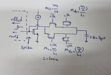
I designed a circuit and I want to sample a voltage at a node(vgs) Corresponding to the previous stage in the period of the time and keep it for a short time
when I use the complementary switch with dummy due to clock-feedthrough it creates spike in transition clock in the previous stage and i have to choose big CH
how can i cancel these spike
what kind of model switch (complementary, bootstrapped,... ) are suitable for sample and hold circuit
 

You want an analog CMOS switch specified for low coupling capacitance from the control signal to the conducting channel.
Analog Devices, TI, and Maxim are good places to look for such switches.
 

Maybe it is a good idea to show your circuit and simulation results so we know what you are talking about. Otherwise, you will just get general comments as reply.
 

Equal-sized CMOS switch may give a low charge injection
at a particular point in the common mode range but as you
depart from the balance-point you will see charge injection
increase. A small a switch as can meet the acquisition /
sample-mode settling time, is best for charge injection.

A lower-overdrive switch gate drive circuit can also help,
but now you need some extra circuitry to make a "local rail
pair" with "just enough headroom" for wherever the input
is sitting. That would then limit ability to track high frequency
inputs (which may or may not be a valid application case).

Last time I designed a S/H piece-part, I was on a JFET
technology and had to make a low-gate-swing drive, plus
add a compensating device counter-switching to minimize
the sampling pedestal. That's all hand-tune-y type work, to
be repeated once you get an extracted layout.
 

Untitled.png
--- Updated ---

a way to remove the spike (cuase clock-feedthrough charge) from Previous stage
Previous stage has small capacitance(cgs) because of this so it is affected by the capacitive coupling
 
Last edited by a moderator:

From your original and rather vague premise, I would suggest a Boot-Strapped Switch for sampling your signal.
Bootstrapping allows the switch itself to be of minimal size since it always gets full VGS. And hence your parasitic caps are also minimal reducing the amount of clock feed-through.
 

Status
Not open for further replies.

Part and Inventory Search

Welcome to EDABoard.com

Sponsor

Back
Top