Continue to Site

Welcome to EDAboard.com

Welcome to our site! EDAboard.com is an international Electronics Discussion Forum focused on EDA software, circuits, schematics, books, theory, papers, asic, pld, 8051, DSP, Network, RF, Analog Design, PCB, Service Manuals... and a whole lot more! To participate you need to register. Registration is free. Click here to register now.

What is the connection technique of conductive paths and SMD materials in this circuit?

Status
Not open for further replies.

bunalmis

Full Member level 5
Joined
Jan 3, 2003
Messages
276
Helped
19
Reputation
38
Reaction score
13
Trophy points
1,298
Location
Ireland
Activity points
2,161
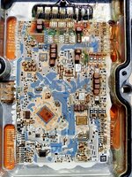
Circuit.jpg

Wire bonding technique is used for the chips and connectors, but what about the others?

How are the conductive paths made in the circuit in the photo?

How are the smd resistor, capacitors and paths connected?

The conductive parts of the smd resistor and capacitors are painted with a brown object. What is this brown object?
 
Last edited by a moderator:


As described by KlausST, thick film hybrid circuit, Al2O3 substrate, AgPd conductor ink (may optionally use Au for circuits involving Au bond wires), glass insulation, fired in protective atmosphere. Mostly uses regular reflow soldering for SMD components, in some cases conductive epoxy.
--- Updated ---

As far as I'm aware of, the shown circuit doesn't use SMD resistors, only printed thick film resistors, some of them laser trimmed.
 
Last edited:
Status
Not open for further replies.

Part and Inventory Search

Welcome to EDABoard.com

Sponsor

Back
Top