Welcome to our site! EDAboard.com is an international Electronics Discussion Forum focused on EDA software, circuits, schematics, books, theory, papers, asic, pld, 8051, DSP, Network, RF, Analog Design, PCB, Service Manuals... and a whole lot more! To participate you need to register. Registration is free. Click here to register now.
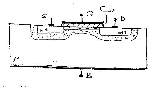
The basic structure of MOS (Metal-Oxide-Semiconductor) forms a capacitor.
To explain qualitatively, consider that a current is flowing in the semiconductor. Now we have the scenario that there is an insulating medium (oxide layer) in between two conducting media (metal is the other). This is similar to a parallel plate capacitor.
In MOSFETs, the current in the semiconductor is established when a channel is present below the gate region. In this scenario, the capacitance is the maximum and this can be utilized effectively.
For a detailed quantitative description and a field theory perspective analysis, refer to the book "The MOS Transistor" by Yannis Tsividis..
This site uses cookies to help personalise content, tailor your experience and to keep you logged in if you register.
By continuing to use this site, you are consenting to our use of cookies.