Continue to Site

Welcome to EDAboard.com

Welcome to our site! EDAboard.com is an international Electronics Discussion Forum focused on EDA software, circuits, schematics, books, theory, papers, asic, pld, 8051, DSP, Network, RF, Analog Design, PCB, Service Manuals... and a whole lot more! To participate you need to register. Registration is free. Click here to register now.

Voltage follower/buffer with op-amp

Status
Not open for further replies.

grieih

Newbie
Joined
Dec 11, 2021
Messages
3
Helped
0
Reputation
0
Reaction score
1
Trophy points
3
Activity points
44
Hi,

I'm trying to build a simple voltage follower using a TL072IP op-amp I got, just for learning purposes. Something similar to this (image from Wikipedia):

1639262578643.png


Here we can see the inputs/outputs for the amplifier according to the vendor's datasheet:

1639262777677.png


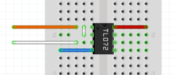
And this is the circuit I came up with:

1639263075824.png


However, no matter what I connect "IN+" to (5V or 0) the output is always the same: ~4.64V. I expected to have either 5V or 0 at the output. If I left the input floating, the output goes down to ~1.5V.

I tried to make sure the connections are OK, read the datasheet, and also tried using the second op-amp from the package (as this part is a dual one) but the result is the same.

Can anybody help me understanding this circuit? What am I doing wrong?

Thanks in advance.
 

Attachments

  • 1639263056313.png
    1639263056313.png
    47.7 KB · Views: 150

Hi,

An Opamp is an Opamp, it is designed for amplifying analog signals.
Neither input nor output should go close to the supply rails (some newer devices so called "rail to rail" are designed to improve on this)

For the TL072 the recommended input voltage range is
* VCC- + 2V = GND +2 = 2V
* VCC+ + 0.1 = 5V + 0.1V = 5.1V

The output is limited to
* VCC- + 0.115V = 0.115V
* VCC+ - 0.105V = 4.895V

Thus you violate the specified area. When you do this the output is not "close to the expected", it even may go anywhere. It is undefined.

I don't know what you want to achieve
Signals close to the rails are typical for CMOS logic signals. Maybe you don't need an Opamp at all.

Klaus

Added:
* Your example design misses fast power supply decoupling capacitor(s)
* Don't leave input signal floating. Neither of the used Opamp, nor for the (second) unused Opamp. Neither for analog ICs, nor for digital ICs.
 
Last edited:

    grieih

    Points: 2
    Helpful Answer Positive Rating
As pointed out by Klaus you are violating CM input range, and the output is
not rail to rail either.

1639279680049.png


Regards, Dana.
 

TL072 isn't known to show gain reversal, also the simulated buffer has monotonic behaviour. In so far the results in post #1 are not entirely plausible. I wonder if its a genuine TI part. It should be however mentioned that the datasheet doesn't cover behaviour below 8V supply voltage.
 

From the datasheet -
1639307007587.png


And specs start with -

1639307102589.png


But as a jfet part its crappy part to use as a single 5V supply OpAmp....


Regards, Dana.
 

Thank you for your replies!

I don't know what you want to achieve
Signals close to the rails are typical for CMOS logic signals. Maybe you don't need an Opamp at all.
I've never worked with opamps before, so I started reading some books and one of the first application circuits with opamps is the voltage follower or buffer, to have an output signal with the same amplitude as the input. I overlooked the part that says the recommended input voltage, for my setup, would be 2V (I only looked at the absolute maximum ratings, that is VCC- -0.5 and VCC+ +0.5 if I'm not wrong) so I understand that a different opamp, with different ratings and input voltages, would be needed if one wanted to create a voltage follower with a wider input range that could be used for digital signals at 0 and 5V, right?

TL072 isn't known to show gain reversal, also the simulated buffer has monotonic behaviour. In so far the results in post #1 are not entirely plausible. I wonder if its a genuine TI part. It should be however mentioned that the datasheet doesn't cover behaviour below 8V supply voltage.
I got it from Mouser, and I think it shows the TI logo, but I'm not sure how could I check if it is genuine or not. By the way, in the datasheet, I could read in the first page that the supply voltage was "±2.25 V to ±20 V, 4.5 V to 40 V". Where could you see this reference to the 8V supply voltage?

Regards.
 

Hi,
I understand that a different opamp, with different ratings and input voltages, would be needed if one wanted to create a voltage follower with a wider input range that could be used for digital signals at 0 and 5V, right?
An Opamp isn't designed for digital signals at all. Neither input, nor output. They are designed for analog input and analog output.
If you want analog input and digital output, then look for a comparator.
If you want digital input and digital output look for digital logic circuits.
If you want digital input and analog output, look for DAC, filters..

Some use Opamps for the function of a comparator. Some Opamps can handle this, but many Opamps don't work very good for this. Some don't work, some even get killed when you apply large differential input voltage. Thus I generally recommend Opamps for purely analog circuits and comparators for digital output circuits.

Opamps:
* are designed that the output always stays within the linear region between bith supply rails.
* are designed that the differential input is always very close to zero.

Comparators:
* can handle large differential input voltage
* are designed for the output to switch to either 'LOW / OPEN' (open emitter, open source) or ' LOW / HIGH' (push pull, totem pole)

Klaus
 

Thanks to danadakk for showing the updated specifications in recent TL072 datasheet. I was referring to the 1996 revision. Interestingly, the new datasheet also mentions phase reversal below 1 V input, see paragraph 9.3 Unity gain buffer. So everything seems clear now.

1639310377234.png


TL072 phase reversal is not correctly modelled in the TI provided SPICE macro model which abstracts from real current mirror and gain stage topology.
--- Updated ---

I expect that phase reversal can be blocked by providing a series resistor for buffer input. It can limit the current through forward biased JFET gate diode and prevent irregular operation of the current mirror stage.
 
Last edited:
  • Like
Reactions: grieih

    grieih

    Points: 2
    Helpful Answer Positive Rating
Thank you both for your answers.

Note that I'm not trying to build anything from this for real use. I mean, I just don't need to create a buffer myself, I can have a real IC buffer for digital circuits, I'm only learning about operational amplifiers, and the buffer is one of the first circuits those books typically show you. I wanted to understand why it didn't work as I expected (if I wasn't understanding the circuit, or maybe the part I was using, TL072, was not appropriate for this kind of setups) before moving on to more advanced op-amp circuits.

Regards.
 
  • Like
Reactions: FvM

Some useful references -


Regards, Dana.
--- Updated ---

FVM talked about incomplete spice models. Thats unfortunately more true than not.
Many manufacturers protect proprietary IP by not modeling that for general publ;ic.

AS good example is current RRIO technology, crossover distortion in input stages,
few datasheets discuss this. And spice models do not reflect it.


Regards, Dana.
 
Last edited:
The Texas Instruments datasheet dated 2017 recommends a supply that is a minimum of 10V (plus and minus 5V). Its common-mode input limit is 4V above the negative supply which is +4V in your single positive supplied circuit.

Some of them will produce phase reversal if the input is less than +1V in your circuit then the output will go as high as it can which is about 1.5V less than the positive supply.

opamp phase inversion.PNG
 

In case of TL072, there's no hidden IP. The datasheet transistor level circuit is well explaining the observed phase reversal, unfortunately the TI macro model is abstracting from this detail. Device level models have been published e.g. at https://groups.io/g/ltspice
 

Put a 10k pot on the input, across the 5V rail, with wiper to the input of the op-amp

also add 10uF + 100nF right across the supply pins - if the opamp is still OK - the output will now follow the input from the pot - provided you stay within the input DM & CM limits, and within the capability of the op-amp to go near 0v and Vcc ( 5V ) - it can't go very close ....
 

The moral is: always read the data sheet for a pertinent information before using a part.
Many cases of posters complaining that parts or circuits are "not operating as expected" is the result of not doing that.
 
Status
Not open for further replies.

Part and Inventory Search

Welcome to EDABoard.com

Sponsor

Back
Top