Continue to Site

Welcome to EDAboard.com

Welcome to our site! EDAboard.com is an international Electronics Discussion Forum focused on EDA software, circuits, schematics, books, theory, papers, asic, pld, 8051, DSP, Network, RF, Analog Design, PCB, Service Manuals... and a whole lot more! To participate you need to register. Registration is free. Click here to register now.

Verilog Quad 7-seg display

Status
Not open for further replies.

Azaxa

Newbie level 4
Joined
Oct 24, 2014
Messages
6
Helped
0
Reputation
0
Reaction score
0
Trophy points
1
Activity points
95
I am creating a Time-Multiplexed Quad Seven-Segment Display where the last 2 digits of the display, AN2 & AN3, show the decimal value 00-99 from an input of 8 switches (ignoring values at 100+). I have a few examples of code where the output on the display is correct according to ISim but with synthesis errors, another where the synthesis is correct but display values are incorrect. I believe it has something to do with the binary to BCD conversion from analyzing I/O results from all registers in the code (most likely blocking(=)/non-blocking(<=) procedural assignments)

If anyone could lend a hand on this it would be appreciated.


Synthesis works but display is incorrect:


Code Verilog - [expand]
1
2
3
4
5
6
7
8
9
10
11
12
13
14
15
16
17
18
19
20
21
22
23
24
25
26
27
28
29
30
31
32
33
34
35
36
37
38
39
40
41
42
43
44
45
46
47
48
49
50
51
52
53
54
55
56
57
58
59
60
61
62
63
64
65
66
67
68
69
70
71
72
73
74
75
76
77
78
79
80
81
82
83
84
85
86
87
88
89
90
91
92
93
94
95
96
97
98
99
100
101
102
103
104
105
106
107
108
109
110
111
112
113
`timescale 1ns / 1ps
//////////////////////////////////////////////////////////////////////////////////
//////////////////////////////////////////////////////////////////////////////////
module example(
input [7:0]sw,
input clk,reset, d0, d1, d2, d3,
output reg [6:0]seg,
output reg dp 
);
 
reg [7:0] shift; 
reg [3:0]val_out;
reg [3:0]Q;
reg [3:0]val0, val1, val2, val3;
reg clkout;
reg an0,an1,an2,an3;
wire [1:0]s;
integer i;
 
 
always @ (posedge clk)
begin
    if (reset)
    begin
        Q <= 4'b0000;
    end
    else
    if(Q !=4'b1111)
        Q <= Q + 1;
    else
        Q <= 0;
end
 
assign s[1:0] = Q[3:2];
 
always@(s)
begin
an0 = 1;
an1 = 1;
an2 = 1;
an3 = 1;
case({s})
    2'b00: an0 = 0;
    2'b01: an1 = 0;
    2'b10: an2 = 0;
    2'b11: an3 = 0;
    default: {an0, an1, an2, an3} = 1;
endcase
end
 
always @(s)
begin
    case (s)
        2'b00: dp = d0;
        2'b01: dp = d1;
        2'b10: dp = d2;
        2'b11: dp = d3;
        default: dp = 1'b1;
    endcase
end
 
always @(s) 
begin
    case (s)
        2'b00: val_out[3:0] = val0[3:0];
        2'b01: val_out[3:0] = val1[3:0];
        2'b10: val_out[3:0] = val2[3:0];
        2'b11: val_out[3:0] = val3[3:0];
        default:val_out[3:0] = 4'b0000;
    endcase
end
 
always @(val_out[3:0])
begin
    case(val_out[3:0])
        4'h0: seg = 7'b0000001;
        4'h1: seg = 7'b1001111;
        4'h2: seg = 7'b0010010;
        4'h3: seg = 7'b0000110;
        4'h4: seg = 7'b1001100;
        4'h5: seg = 7'b0100100;
        4'h6: seg = 7'b0100000;
        4'h7: seg = 7'b0001111;
        4'h8: seg = 7'b0000000;
        4'h9: seg = 7'b0000100;
        default:seg = 7'b1111111; 
    endcase
end
 
always @(sw[7:0])
 begin  
 
    shift[7:0] = sw[7:0];
    
 for (i=0; i<7; i=i+1)
    begin
        if (shift[3:0] >= 5)
             shift[3:0] = shift[3:0] + 3;
        if (shift[7:4] >= 5)
             shift[7:4] = shift[7:4] +3;
            
        shift = shift << 1;
 
    end 
    
    val3[3:0] <= shift[7:4];
    val2[3:0] <= shift[3:0];
    val1[3:0] <= 4'b0100;
    val0[3:0] <= 4'b0110;
    
end
 
endmodule


Display is correct but Synthesis doesn't work giving an error

ERROR:Xst:880 - "example.v" line 102: Cannot mix blocking and non blocking assignments on signal <shift>.
ERROR:Xst:880 - "example.v" line 98: Cannot mix blocking and non blocking assignments on signal <shift>.


Code Verilog - [expand]
1
2
3
4
5
6
7
8
9
10
11
12
13
14
15
16
17
18
19
20
21
22
23
24
25
26
27
28
29
30
31
32
33
34
35
36
37
38
39
40
41
42
43
44
45
46
47
48
49
50
51
52
53
54
55
56
57
58
59
60
61
62
63
64
65
66
67
68
69
70
71
72
73
74
75
76
77
78
79
80
81
82
83
84
85
86
87
88
89
90
91
92
93
94
95
96
97
98
99
100
101
102
103
104
105
106
107
108
109
110
111
112
113
`timescale 1ns / 1ps
//////////////////////////////////////////////////////////////////////////////////
//////////////////////////////////////////////////////////////////////////////////
module example(
input [7:0]sw,
input clk,reset, d0, d1, d2, d3,
output reg [6:0]seg,
output reg dp 
);
 
reg [7:0] shift; 
reg [3:0]val_out;
reg [3:0]Q;
reg [3:0]val0, val1, val2, val3;
reg clkout;
reg an0,an1,an2,an3;
wire [1:0]s;
integer i;
 
 
always @ (posedge clk)
begin
    if (reset)
    begin
        Q <= 4'b0000;
    end
    else
    if(Q !=4'b1111)
        Q <= Q + 1;
    else
        Q <= 0;
end
 
assign s[1:0]= Q[3:2];
 
always@(s)
begin
an0 = 1;
an1 = 1;
an2 = 1;
an3 = 1;
case({s})
    2'b00: an0 = 0;
    2'b01: an1 = 0;
    2'b10: an2 = 0;
    2'b11: an3 = 0;
    default: {an0, an1, an2, an3} = 1;
endcase
end
 
always @(s)
begin
    case (s)
        2'b00: dp = d0;
        2'b01: dp = d1;
        2'b10: dp = d2;
        2'b11: dp = d3;
        default: dp = 1'b1;
    endcase
end
 
always @(s) 
begin
    case (s)
        2'b00: val_out[3:0] = val0[3:0];
        2'b01: val_out[3:0] = val1[3:0];
        2'b10: val_out[3:0] = val2[3:0];
        2'b11: val_out[3:0] = val3[3:0];
        default:val_out[3:0] = 4'b0000;
    endcase
end
 
always @(val_out[3:0])
begin
    case(val_out[3:0])
        4'h0: seg = 7'b0000001;
        4'h1: seg = 7'b1001111;
        4'h2: seg = 7'b0010010;
        4'h3: seg = 7'b0000110;
        4'h4: seg = 7'b1001100;
        4'h5: seg = 7'b0100100;
        4'h6: seg = 7'b0100000;
        4'h7: seg = 7'b0001111;
        4'h8: seg = 7'b0000000;
        4'h9: seg = 7'b0000100;
        default:seg = 7'b1111111; 
    endcase
end
 
always @(sw[7:0])
 begin  
 
    shift[7:0] = sw[7:0];
    
 for (i=0; i<7; i=i+1)
    begin
        if (shift[3:0] >= 5)
             shift[3:0] <= shift[3:0] + 3;
        if (shift[7:4] >= 5)
             shift[7:4] <= shift[7:4] +3;
            
        shift <= shift << 1;
 
    end 
    
    val3[3:0] = shift[7:4];
    val2[3:0] = shift[3:0];
    val1[3:0] = 4'b0100;
    val0[3:0] = 4'b0110;
    
end
 
endmodule


Both using this test bench/text fixture.


Code Verilog - [expand]
1
2
3
4
5
6
7
8
9
10
11
12
13
14
15
16
17
18
19
20
21
22
23
24
25
26
27
28
29
30
31
32
33
34
35
36
37
38
39
40
41
42
43
44
45
46
47
48
49
50
51
52
53
54
55
56
57
58
59
60
61
62
63
64
65
66
67
68
69
70
71
72
73
74
75
76
77
78
`timescale 1ns / 1ps
 
 module exampletb;
 
 // Inputs
 reg clk;
 reg reset;
 reg d0;
 reg d1;
 reg d2;
 reg d3;
 reg [7:0]sw;
 
 // Outputs
 wire [3:0] Q;
 wire [3:0] val0;
 wire [3:0] val1;
 wire [3:0] val2;
 wire [3:0] val3;
 wire [6:0] seg;
 wire dp;
 wire an0;
 wire an1;
 wire an2;
 wire an3;
 wire [7:0]shift;
 wire [3:0] val_out;
 
 // Instantiate the Unit Under Test (UUT)
 example uut (
 .clk(clk),
 .reset(reset),
 .d0(d0),
 .d1(d1),
 .d2(d2),
 .d3(d3),
 .seg(seg),
 .dp(dp),
 .sw(sw)
 );


 always
    #10 clk = ~clk;
 
 initial
 begin
  clk = 1'b1;
 reset = 1'b1;
 #110;
 reset = 1'b0;
 end
 
 initial begin
 $display("If simulation ends prematurely, restart");
 $display("using 'run -all' on the command line.");
 // This should get "3 2.1 0." on the display.
 d3 <= 1'b0;
 d2 <= 1'b1;
 d1 <= 1'b0;
 d0 <= 1'b1;
 
 sw <= 8'h23;
 #300
 sw <= 8'h22;
 #320
 sw <= 8'h21;
 #320
 sw <= 8'h20;
 #320
 sw <= 8'h19;
 #320
 sw <= 8'h18;
 #320
 sw <= 8'h17;
 
endmodule


P.S. if you can understand why the binary to BCD converter produces the correct BCD value on the display using hexadecimal switch input values when it should be working with decimal instead that would be helpful; using the second program example. Thanks in advance. :)

S.D.
 

I think I recognize that code. It looks like that code that was posted recently in another thread, where there were a number of suggestions made to improve it. I actually thought it should have been redone, so I reduced the size of it and made it fully synchronous. I would suggest you start with something else that is not from that poster.

Sure I could post my improved version, but then you would lose any kind of learning opportunity gained by doing your homework assignment on your own. :)
 

This was done completely on my own through exercises from University :S but if that's the case I can see why you'd think that. Thanks anyway
 

Well in that case...

Code Verilog - [expand]
1
2
3
4
always @ (posedge clk)
begin
  // all your code should be inside here
end


As a beginner I would avoid large combinational blobs generating every output of your circuit.


Code Verilog - [expand]
1
2
3
4
5
6
7
8
9
10
11
12
13
14
15
16
17
18
19
20
21
22
always @(sw[7:0])
 begin  
 
    shift[7:0] = sw[7:0];
    
 for (i=0; i<7; i=i+1)
    begin
        if (shift[3:0] >= 5)
             shift[3:0] <= shift[3:0] + 3;
        if (shift[7:4] >= 5)
             shift[7:4] <= shift[7:4] +3;
            
        shift <= shift << 1;
 
    end 
    
    val3[3:0] = shift[7:4];
    val2[3:0] = shift[3:0];
    val1[3:0] = 4'b0100;
    val0[3:0] = 4'b0110;
    
end


This is pretty much a rewrite. You've got a mix of <= (non-blocking) and = blocking in a combinational description. You've assigned sw using a blocking statement, and your latch design is assigning shift using non-blocking statements. I don't think this would even work in an FPGA after you fix the non-blocking assignments (you shouldn't be using them in a combinational always block).
Anytime you have a feedback path there better be a flip-flop in the path, otherwise you'll end up with latches in the design.

I think you're biggest problem is you didn't do any up front design (like drawing a block diagram) and then drawing detailed block diagrams of the major blocks before writing your code. This code looks more like software than a hardware implementation. If you know what your hardware implementation looks like then the RTL (Regiter Transfer Level) description is easy to write.

Regards
 

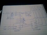
Ah right. Analyzing my code it looks like this is what i'm doing from a block diagram perspective.

2014-10-24 23-57-32.199.jpg

Placing the always block in the entire circuit causes errors with the other always@ blocks inside of the "always@ (posedge clk)" block. And I used the binary-BCD code on the second example for using non-blocking on the shift and if 5 then +3 parts. I will attempt a different design but from the material we have covered there's only so many ways I can reformat the code (I've tried many to finally get this one working). I'll try again and post how it goes tomorrow :) thanks.
 

register the output of your decoders, it will keep the outputs from glitching.
 

I tried a few variations of formatting the blocking/non-blocking assignments and all of the outputs are registers including the output from the decoders but the same error persists
Code:
ERROR:Xst:528 - Multi-source in Unit <test> on signal <val0<3>>; this signal is connected to multiple drivers.
ERROR:Xst:528 - Multi-source in Unit <test> on signal <val0<2>>; this signal is connected to multiple drivers.
ERROR:Xst:528 - Multi-source in Unit <test> on signal <val0<1>>; this signal is connected to multiple drivers.
ERROR:Xst:528 - Multi-source in Unit <test> on signal <val0<0>>; this signal is connected to multiple drivers.
ERROR:Xst:528 - Multi-source in Unit <test> on signal <val1<3>>; this signal is connected to multiple drivers.
ERROR:Xst:528 - Multi-source in Unit <test> on signal <val1<2>>; this signal is connected to multiple drivers.
ERROR:Xst:528 - Multi-source in Unit <test> on signal <val1<1>>; this signal is connected to multiple drivers.
ERROR:Xst:528 - Multi-source in Unit <test> on signal <val1<0>>; this signal is connected to multiple drivers.
ERROR:Xst:528 - Multi-source in Unit <test> on signal <val2<3>>; this signal is connected to multiple drivers.
ERROR:Xst:528 - Multi-source in Unit <test> on signal <val2<2>>; this signal is connected to multiple drivers.
ERROR:Xst:528 - Multi-source in Unit <test> on signal <val2<1>>; this signal is connected to multiple drivers.
ERROR:Xst:528 - Multi-source in Unit <test> on signal <val2<0>>; this signal is connected to multiple drivers.
ERROR:Xst:528 - Multi-source in Unit <test> on signal <val3<3>>; this signal is connected to multiple drivers.
ERROR:Xst:528 - Multi-source in Unit <test> on signal <val3<2>>; this signal is connected to multiple drivers.
ERROR:Xst:528 - Multi-source in Unit <test> on signal <val3<1>>; this signal is connected to multiple drivers.
ERROR:Xst:528 - Multi-source in Unit <test> on signal <val3<0>>; this signal is connected to multiple drivers.


Code:
`timescale 1ns / 1ps
///////////////////////////////////////////////////////////
module test(

input [7:0]sw,
input clk,reset, d0, d1, d2, d3,
output reg [3:0]val0, val1, val2, val3,
output reg [6:0]seg,
output reg dp,
output reg [7:0] shift,
output reg [3:0]Q,
output reg [1:0]s,
output reg clkout,
output reg an0,an1,an2,an3
);

reg [3:0]val_out;
integer i;

//		 0
//		___
//	5 |	| 1
//   | 6 |
//		---
//	  |	| 
//	4 |___| 2
//		 3

always @(posedge clk)
begin	
	if (reset)
		begin
		clkout <= 0;
		val0 <= 4'b0000;
		val1 <= 4'b0000;
		val2 <= 4'b0000;
		val3 <= 4'b0000;
		Q <= 0;
		s <= 0;
		end
	else
		if (Q != 4'b1111)
			begin
			Q <= Q + 1;
			clkout <= 0;
			s <= 0;
			end
		else
			begin
			Q <= 0;
			clkout <= 1;	
			end
		if (clkout != 1)
			s <= s;
		else
			begin
				if (s != 2'b11)
					s <= s + 1;
				else
					s <= 0;		
			end
		
an0 <= 1;
an1 <= 1;
an2 <= 1;
an3 <= 1;
case({s})
	2'b00: an0 <= 0;
	2'b01: an1 <= 0;
	2'b10: an2 <= 0;
	2'b11: an3 <= 0;
	default: {an0, an1, an2, an3} <= 1;
endcase

	case (s)
		2'b00: dp <= d0;
		2'b01: dp <= d1;
		2'b10: dp <= d2;
		2'b11: dp <= d3;
		default: dp <= 1'b1;
	endcase

	case (s)
		2'b00: val_out[3:0] <= val0[3:0];
		2'b01: val_out[3:0] <= val1[3:0];
		2'b10: val_out[3:0] <= val2[3:0];
		2'b11: val_out[3:0] <= val3[3:0];
		default:val_out[3:0] <= 4'b0000;
	endcase

	case(val_out[3:0])
		4'h0: seg <= 7'b0000001;
		4'h1: seg <= 7'b1001111;
		4'h2: seg <= 7'b0010010;
		4'h3: seg <= 7'b0000110;
		4'h4: seg <= 7'b1001100;
		4'h5: seg <= 7'b0100100;
		4'h6: seg <= 7'b0100000;
		4'h7: seg <= 7'b0001111;
		4'h8: seg <= 7'b0000000;
		4'h9: seg <= 7'b0000100;
		default:seg <= 7'b1111111; 
	endcase
end

always@ (sw)
begin
    shift[7:0] = sw[7:0];
    
 for (i=0; i<7; i=i+1)
    begin
        if (shift[3:0] >= 5)
             shift[3:0] = shift[3:0] + 3;
        if (shift[7:4] >= 5)
             shift[7:4] = shift[7:4] +3;
            
        shift = shift << 1;
 
    end 
    
    val3[3:0] = shift[7:4];
    val2[3:0] = shift[3:0];
    val1[3:0] = 4'b0100;
    val0[3:0] = 4'b0110;
end   
endmodule

P.S. I removed the always@ (sw) and placed it all in the always@ (posedge clk) block which i believe removed the multi-source error but gave the exact same errors as example 1 and 2 in the first post. It's a problem with the procedural assignments on the shift register but any procedural assignment combination for the shift register results in either a bad synthesis but correct ISim simulation when non-blocking assignments are used in the for loop, producing error:

Code:
    shift[7:0] = sw[7:0];
    
 for (i=0; i<7; i=i+1)
    begin
        if (shift[3:0] >= 5)
             shift[3:0] <= shift[3:0] + 3;
        if (shift[7:4] >= 5)
             shift[7:4] <= shift[7:4] +3;
            
        shift <= shift << 1;
 
    end 
    
    val3[3:0] = shift[7:4];
    val2[3:0] = shift[3:0];
    val1[3:0] = 4'b0100;
    val0[3:0] = 4'b0110;

ERROR:Xst:880 - "test.v" line 121: Cannot mix blocking and non blocking assignments on signal <shift>.

Or a good synthesis but with 0 values produced at val3 and val2 when all blocking assignments are used

Code:
    shift[7:0] = sw[7:0];
    
 for (i=0; i<7; i=i+1)
    begin
        if (shift[3:0] >= 5)
             shift[3:0] = shift[3:0] + 3;
        if (shift[7:4] >= 5)
             shift[7:4] = shift[7:4] +3;
            
        shift = shift << 1;
 
    end 
    
    val3[3:0] = shift[7:4];
    val2[3:0] = shift[3:0];
    val1[3:0] = 4'b0100;
    val0[3:0] = 4'b0110;
 

I don't think you understand for loops in Verilog. I also think you need to review your blocking and non-blocking assignment topics. You don't seem to understand that you should never use blocking assignments in a edge triggered always block (i.e. clocked) and you should never use non-blocking assignments in a combinational always block. Of course the language allows you do mix them, but there are good reasons not to.

Any synthesizable circuit can be designed if you stick with the following rules:
1. Edge triggered always blocks => use non-blocking assignments (<=)
2. Combinational always blocks => use blocking assignments (=)
There is no need to use a mixed approach or use the other assignment type. In many cases you can have errors for the mixed approach or mismatches in simulation/synthesis and in the second case you could have potential simulation/synthesis mismatches depending on your code as non-blocking and blocking assignments have a differing order of evaluation.

I think you should also study about for loops in Verilog, they aren't the same as for loops in software languages like C/C++. For loops in Verilog are used to replicated logic.


Code Verilog - [expand]
1
2
3
4
5
6
7
8
9
10
11
shift[7:0] = sw[7:0];  //this is a blocking assignment to [B]shift[/B]
    
 for (i=0; i<7; i=i+1)
    begin
        if (shift[3:0] >= 5)
             shift[3:0] <= shift[3:0] + 3;  // now you are using non-blocking assignments for [B]shift[/B]
        if (shift[7:4] >= 5)
             shift[7:4] <= shift[7:4] +3;  // you can't mixed assignment types for the same signal
            
        shift <= shift << 1;           // that is why you are getting the error: 
                                       // ERROR:Xst:880 - "test.v" line 121: Cannot mix blocking and non blocking assignments on signal <shift>.


I removed the always@ (sw) and placed it all in the always@ (posedge clk)
Without testing it myself changing the block from combinational to edge triggered and still using the blocking assignments is probably causing the problem with the updates to shift. You should avoid using any for loops until you understand what kind of logic they generate.

IMO, your design for this is overly complicated and not at all easy to follow. I'm not sure but from your original description you are trying to convert an 8-bit switch setting to a two digit number from 00-99, i.e 8'd00-8'd99. Now it's not apparent if the 8-bit number is BCD or binary. If it's binary you should have first converted it to BCD and then displayed it. If the crazy shift thing is supposed to convert binary to BCD, I can't tell.
 

A variable can't be assigned in more than one always block or concurrent statement.
val0 to val3 are set in the combinational always block (the double dabble binary to decimal converter). So you need to comment the reset initialization in the other block.

Then your code will compile without errors.

I don't think you understand for loops in Verilog. I also think you need to review your blocking and non-blocking assignment topics. You don't seem to understand that you should never use blocking assignments in a edge triggered always block (i.e. clocked) and you should never use non-blocking assignments in a combinational always block.

The latest code has no problems in this regard. The combinational for loop is a correct behavioral description of a binary-to-decimal converter. In this case, the for loop is enrolled to a moderate amount of synthesized logic. This might end up different in other cases. For a larger word size, a clocked sequential design might be preferable.

If the crazy shift thing is supposed to convert binary to BCD, I can't tell.
It actually does. See https://en.wikipedia.org/wiki/Double_dabble
 

The your code is working.

Maybe working, but I sure wouldn't want it deployed in a product.

I'd really like to see people come in for an interview that can actually write good VHDL/Verilog code, without all the issues I see everyday on this forum. Most of the interviewees we've seen in the past 3 months all seem to have a similar level of expertise in RTL coding as the majority of newbie posters to this forum. Hence my tendency to try and get those newbies to actually learn how to write better code. Not just write code that "works".
 

As far as I see, the OP essentially implemented your suggestions about blocking and non-blocking statements and put most of the code into the clocked always block.

The combinational decimal converter is a special case. If you analyze the synthesis results, you probably have to admit that it's a quite effective parallel implementation.
 

As far as I see, the OP essentially implemented your suggestions about blocking and non-blocking statements and put most of the code into the clocked always block.
Okay that's true, but I still think there's a simpler solution, but maybe not (I really don't have the time to analyze it) I'm only doing this while my simulation and builds run.
The combinational decimal converter is a special case. If you analyze the synthesis results, you probably have to admit that it's a quite effective parallel implementation.
Myabe so but I don't have the time to analyze it, besides I've designed and have seen much easier to see/understand versions of similar circuits.

Simplicity has it's own elegance. Of course that is just my opinion.
 

There's at least one detail that has to be improved. The segment output is delayed relative to s by two clocks. It should be updated synchronously.

There are different ways to fix this problem, one would be to use more combinational and less clocked code...
 

I have to supplement that the BCD encoder code isn't correct. It tries to perform the "double dabble" algorithm in place, which doesn't work because it applies a twofold correction. Review the Wikipedia article for reference.


Code Verilog - [expand]
1
2
3
4
5
6
7
8
9
10
11
12
13
14
15
16
17
18
19
20
21
22
23
24
25
26
module bin2dec(
 
input [7:0]bin,
output reg [3:0]d1,d2
);
 
reg [15:0] shift;
integer i;
 
always@ (*)
begin
    shift[7:0] = bin;
    shift[15:8] =8'b0; 
 for (i=0; i<8; i=i+1)
    begin
        if (shift[11:8] >= 5)
             shift[11:8] = shift[11:8] + 4'd3;
        if (shift[15:12] >= 5)
             shift[15:12] = shift[15:12] +4'd3;
        shift = shift << 1;
    end 
    
    d2[3:0] = shift[15:12];
    d1[3:0] = shift[11:8];
end   
endmodule


Simplicity has it's own elegance.
Hard to disagree. I wonder how an elegant BCD encoder would look like. The examples in literature said to be effective (e.g. in the Quartus advanced synthesis cookbook) are table driven and even less elegant than double dabble.
 

Thank you for the advice. I implemented the combinational logic as opposed to a purely clocked system and that has solved the issue where the 7-seg displays 2 clk cycles after s. I'm not entirely sure why it now accepts that there are no multiple drives for val2/3 as they are both in separate always blocks (one for binary to BCD) and one for case(s) 2'b00: val_out = val3; etc.

Regardless, it simulates perfectly now and the synthesis appears to be fine. So, once again, thanks for the advice it's really helped understanding how Verilog behaves.

Working Code:

Code:
`timescale 1ns / 1ps
///////////////////////////
module Time_Multiplexed_Quad_7_Seg_Display(
//Inputs
input [7:0]sw,
input clk,reset, dot0, dot1, dot2, dot3,

//Outputs
output reg [6:0]seg,
output reg dp,
output reg [3:0]val_out,
output reg an0,an1,an2,an3,
output reg [15:0]shift,
output reg [3:0]Q,
output reg [1:0]s,
output reg [3:0]val0, val1, val2, val3,
output reg clkout
);


integer i;

always @(posedge clk)
begin	

//50MHz to 100Hz clock divider
	if (reset) //reset parameters
		begin
		clkout <= 0;
		Q <= 0;
		s <= 0;
		end
	else //if reset = 0 then
	begin
		if (Q != 4'b1111) //when counter is not at maximum value
			begin
			Q <= Q + 1; //add 1 to the counter value
			clkout <= 0; 
			end
		else //when counter is at maximum value
			begin
			Q <= 0; //reset counter
			clkout <= 1; //output the clk divider
			end
		if (clkout != 1) //when clk divider is OFF 
			s <= s; //select bits stay the same
		else //when clk divider is ON
			begin
				if (s != 2'b11) //if select is not at maximum value
					s <= s + 1; //increment select
				else 
					s <= 0; //otherwise reset select		
			end
	end
end
	
always @(s)
begin	//2-4 decoder for digit select		
an0 <= 1;
an1 <= 1; //Active LOW digit select on display
an2 <= 1; //initially set to 1 (OFF)
an3 <= 1;
case({s})
	2'b00: an0 <= 0;
	2'b01: an1 <= 0; //Turn digits ON dependant on
	2'b10: an2 <= 0; //select, [1:0]s, value
	2'b11: an3 <= 0;
	default: {an0, an1, an2, an3} <= 1;
endcase
end 

always @(s)
begin
//4-1 Multiplexer for decimal point for display
	case (s)
		2'b00: dp = dot0;
		2'b01: dp = dot1; //decimal point is assigned to 
		2'b10: dp = dot2; //d0-3 values (from text fixture)
		2'b11: dp = dot3; //for display's decimal point (active LOW)
		default: dp = 1'b1;
	endcase
end

always @(s)
begin
//4-1 Multiplexer for undecoded decimal values for display
	case (s)
		2'b00: val_out[3:0] = val0[3:0]; 
		2'b01: val_out[3:0] = val1[3:0]; //Values given from binary to BCD
		2'b10: val_out[3:0] = val2[3:0]; //converter are assigned to val_out bus
		2'b11: val_out[3:0] = val3[3:0]; //in decimal format to be decoded by [7:0]seg
		default:val_out[3:0] = 4'b0000;
	endcase
end

always @(val_out)
begin	
//4-7 decoder for decoded decimal values for display
	case(val_out[3:0])
		4'h0: seg <= 7'b0000001; //decoded values of decimal value val_out
		4'h1: seg <= 7'b1001111; //suitable for 7-seg display format (a,b,c,d,e,f,g)
		4'h2: seg <= 7'b0010010; //(active LOW)
		4'h3: seg <= 7'b0000110;
		4'h4: seg <= 7'b1001100;
		4'h5: seg <= 7'b0100100;
		4'h6: seg <= 7'b0100000;
		4'h7: seg <= 7'b0001111;
		4'h8: seg <= 7'b0000000;
		4'h9: seg <= 7'b0000100;
		default:seg <= 7'b1111111; 
	endcase
end

always @(sw[7:0])
 begin	
	 shift[15:8] = 8'b0;  //initialise 8 MSB of shift reg to equal 0
	 shift[7:0]  = sw[7:0]; //let input sw equal 8 LSB of shift reg
    	 
 for (i=0; i<8; i=i+1) //loop for integer i equals 0 to 7
    begin
        if (shift[11:8] >= 5) //if units column is greater than 5
             shift[11:8] = shift[11:8] + 4'd3; //add 3 to units column
        if (shift[15:12] >= 5) //if tens column is greater than 5
             shift[15:12] = shift[15:12] +4'd3; //add 3 to tens column
        shift = shift << 1; //then shift the binary value of shift left by one
    end 
    
    val3[3:0] = shift[15:12]; //tens value for digit AN3
    val2[3:0] = shift[11:8]; //units value for digit AN2
	 val1[3:0] = 4'b0100; //decimal value 4 for digit AN1
    val0[3:0] = 4'b0110; //decimal value 6 for digit AN0
	
end

endmodule

and equivalent text fixture/test bench

Code:
`timescale 1ns / 1ps

module testtb;

	// Inputs
	reg [7:0] sw;
	reg clk;
	reg reset;
	reg d0;
	reg d1;
	reg d2;
	reg d3;

	// Outputs
	wire [3:0] val0;
	wire [3:0] val1;
	wire [3:0] val2;
	wire [3:0] val3;
	wire [6:0] seg;
	wire dp;
	wire [3:0] tens;
	wire [3:0] units;
	wire [3:0] val_out;
	wire [3:0] Q;
	wire [1:0] s;
	wire clkout;
	wire an0;
	wire an1;
	wire an2;
	wire an3;

	// Instantiate the Unit Under Test (UUT)
	Time_Multiplexed_Quad_7_Seg_Display uut (
		.sw(sw), 
		.s(s),
		.Q(Q),
		.val_out(val_out),
		.shift(shift),
		.an0(an0),
		.an1(an1),
		.an2(an2),
		.an3(an3),
		.clk(clk), 
		.reset(reset), 
		.dot0(d0), 
		.dot1(d1), 
		.dot2(d2), 
		.dot3(d3), 
		.seg(seg), 
		.dp(dp)
	);


 always
	#10 clk = ~clk;
 
 initial
 begin
 clk = 1'b1;
 reset = 1'b1;
 #100;
 reset = 1'b0;

 end

  always
	#1400 sw = sw + 1;
	
	initial begin

 $display("If simulation ends prematurely, restart");
 $display("using 'run -all' on the command line.");
 // This should get "3 2.1 0." on the display.
 d3 <= 1'b0;
 d2 <= 1'b1;
 d1 <= 1'b0;
 d0 <= 1'b1;
 #100
 sw = 8'd11;
 // Wait until reset is deasserted.
 @(negedge reset);
 $display("Reset is deasserted...");
 $display("Prepare to wait a long time...");
 #5000000;
 $display("Checkpoint, simulation time is %t",$time);
 #5000000;
 $display("Checkpoint, simulation time is %t",$time);
 #5000000;
 $display("Checkpoint, simulation time is %t",$time);
 #5000000;
 $display("Checkpoint, simulation time is %t",$time);
 #5000000;
 $display("Checkpoint, simulation time is %t",$time);
 // End the simulation.
 $display("Simulation is over, check the waveforms.");
 $stop;
 
 
	end
      
endmodule
 

I'm not entirely sure why it now accepts that there are no multiple drives for val2/3 as they are both in separate always blocks (one for binary to BCD) and one for case(s) 2'b00: val_out = val3; etc.
They are driven in only one always block (the BCD encoder).
 

Status
Not open for further replies.

Part and Inventory Search

Welcome to EDABoard.com

Sponsor

Back
Top