Continue to Site

Welcome to EDAboard.com

Welcome to our site! EDAboard.com is an international Electronics Discussion Forum focused on EDA software, circuits, schematics, books, theory, papers, asic, pld, 8051, DSP, Network, RF, Analog Design, PCB, Service Manuals... and a whole lot more! To participate you need to register. Registration is free. Click here to register now.

V-I characteristic curve of parasitic diode on MOSFET

Status
Not open for further replies.

will_fung

Junior Member level 1
Joined
Feb 18, 2014
Messages
17
Helped
0
Reputation
0
Reaction score
0
Trophy points
1,281
Activity points
1,435
I measured the V-I characteristic curve of parasitic diode on MOSFET, seems the slope isn't steep like a diode.

I just use a power supply to power the diode, increase the voltage of power supply, and measure the drop voltage and current flow the diode, then i get the V-I curve.


here is my measurement of V-I curve with a parasitic diode on MOSFET. Is my measurement correct? what's the differences between a diode and a parasitic diode on the V-I curve?
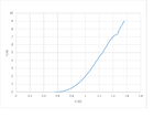
parasitic doide V-I curve.png
 

Any real diode has a certain series resistance, so a MOSFET substrate diode. The shown value of several 100 mOhm suggests that you are either testing a relative small or a high voltage MOSFET. Or the measurement is incorrect.

What's the MOSFET type?
 

First thing first: this is not a real diode, this is a parasitic diode. But the basic principle of operation is the same. We see the same rectification and the broad nature of the curve is same.

For a "real" diode, the y-axis is often logarithmic and the curve is not linear (it is exponential if both the axes are linear).

The diode characteristics depends on the nature of the junction (diffusion layer) and less on the doping material. We see that the slope approx corresponds to 66mOhm resistance. But this MUST be due to several compromises.

But one important thing about measurements: you need to measure at a const junction temp (easy to say but...)

The real difference is that this is an incidental diode and has not been designed optimised.
 

I read it's common for power diodes to drop as much as 1.2 volts or more. The diode has its dynamic (self-altering) resistance, as well as a certain amount of ohmic resistance. The more Amperes you push through it, the greater the voltage drop caused by the ohmic portion. Therefore at high current the ohmic portion becomes more prevalent.

I performed similar tests with ordinary silicon diodes and led's. I plotted the data on graphs. It produced a curve which looked like a cousin of y=x^2. I tried to derive a simple equation to obtain Amperes, given a voltage. I came up with:

A = ( V x 1.25) ^21

Your graph looks like it could be (approximately):

A = (V x 1.1) ^5
 

9A/V is not a bad resistance (100mOhm or so). On a par with
many FETs' on-resistance.

What you see depends all on formatting I think.

At these currents, resistances outside the FET can't be
ignored. Banana jacks and wires alone could be half the
total. I'd look to a Kelvin setup before taking any numbers
seriously.
 

Status
Not open for further replies.

Similar threads

Part and Inventory Search

Welcome to EDABoard.com

Sponsor

Back
Top