Continue to Site

Welcome to EDAboard.com

Welcome to our site! EDAboard.com is an international Electronics Discussion Forum focused on EDA software, circuits, schematics, books, theory, papers, asic, pld, 8051, DSP, Network, RF, Analog Design, PCB, Service Manuals... and a whole lot more! To participate you need to register. Registration is free. Click here to register now.

USB Differential Pair Trace width and Spacing Calculation

Status
Not open for further replies.

Amr Wael

Member level 5
Joined
Jul 13, 2020
Messages
84
Helped
0
Reputation
0
Reaction score
1
Trophy points
8
Activity points
852
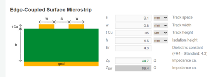
Hello , I am designing a PCB that is featuring USB , I know that the USB traces diff impedance should be 90 ohms. I am planning to manufacture the PCB at PCBWAY so I decided to use their calculator but as you can see in the photo when using the minimum allowed spacing , the width of the traces is so large for usual USB traces. Has anybody faced this problem before? Should I use Saturn PCB or any other calculator or is it better to stick to the manufacturer calculator? I know that there are different formulas and approximations that lead to different numbers but my question is how to solve this issue permanently?
Thank you very much in advance.
 

Attachments

  • Capture.PNG
    Capture.PNG
    25.8 KB · Views: 268

You've got a pretty thick dielectric there. Is this a two-layer board? Normally, you'd have, say, 10 mil height (0.254mm) in a multi-layer board. Different calculators will probably give you slightly different results, but not a lot. You can't change physics.
 

You've got a pretty thick dielectric there. Is this a two-layer board? Normally, you'd have, say, 10 mil height (0.254mm) in a multi-layer board. Different calculators will probably give you slightly different results, but not a lot. You can't change physics.
It's actually a 4 layers board
 

@FvM as @barry said it's just an impedance calculator app on PCBWAY (The manufacturer) and they don't specify the number of layers in the app.
 

That's not the stackup, that's the impedance calculating app.
Yes, and the substrate height is wrong in the calculation input. It's for a 2-layer 1.6 mm board. You should enter the height of the outer layer, presuming you have a ground plane in layer 2.
 

Yes, and the substrate height is wrong in the calculation input. It's for a 2-layer 1.6 mm board. You should enter the height of the outer layer, presuming you have a ground plane in layer 2.
It’s quite possible that the layer spacing is, in fact, 1.6mm. there’s nothing to indicate that the overall board thickness is 1.6mm or 3.2mm or anything else. The OP should verify that they are using the right value, though.
 

Status
Not open for further replies.

Part and Inventory Search

Welcome to EDABoard.com

Sponsor

Back
Top