fouwad
Full Member level 4
hi, i am posting my code as well as my simulation results of ALU, can anyone plz let me know what is causing this unusual simulation results and what can be done to get the desired results.
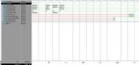
here the results are achieved after quite a number of clockcycles, what in code is responsible for such strange delays
Code:
module ALU( clk,Iid2alu, rs1_data, rs2_data, rd_addr, imm_value, alu_out, rd_data_mem, rd_addr_latched, Ialu2mem

    );

input clk;
 input [0:31] rs1_data;
 input [0:31] rs2_data;
 input [0:4] rd_addr;
 input [0:31]imm_value;
 input [0:31]Iid2alu;
 output reg [0:31]alu_out;
 output reg[0:31]rd_data_mem;
 output reg[0:4]rd_addr_latched;
 output reg [0:7] Ialu2mem;

//g [0:7]csr; // current status register

reg [0:31]alu_result;

reg [0:31]rd_data_mem_val;


reg [0:31] rtype_rslt;
reg [0:31] immtype_rslt;

wire [0:31] A;
wire [0:31] B;
wire [0:31] imm;
wire [0:5] op;
wire [0:4]rd_addr;
wire [0:5] func;

////concatination for 31 to 7 bit reduced values
//assign A={24'b0,rs1_data};
//assign B={24'b0,rs2_data};
//assign imm={24'b0,imm_value};
//


wire [0:31] add_rslt;	//result of addition

wire [0:31] add_rslt_imm; //result of addition with immediate value

wire [0:31] sub_rslt;

wire [0:31] sub_rslt_imm;
//wire [0:32] awc_rslt;

//wire sel_mux; // sel line for mux
wire [0:31] i; // instruction
/*
wire        isLB;		//DATA TRANSFER
wire        isLH;
wire        isLW;
wire        isSB;
wire        isSH;
wire        isSW;
wire        isMOVS2I;
wire        isMOVI2S;

wire        isADD;		//ARTHIMETIC
wire        isADDI;
wire        isSUB;
wire        isSUBI;
wire        isAWC;
wire        isINC;
wire        isDEC;

wire        isAND;		//LOGICAL
wire        isANDI;
wire        isOR;
wire        isORI;
wire        isXOR;
wire        isXORI;

wire        isSLL;		//SHIFT
wire        isSLLI;
wire        isSRL;
wire        isSRLI;

wire 			isCLR;		//TEST SET
wire 			isSET;
wire        isSLT;
wire        isSLTI;
wire        isSGT;
wire        isSGTI;
wire        isSLE;
wire        isSLEI;
wire        isSGE;
wire        isSGEI;
wire        isSEQ;
wire        isSEQI;
wire        isSNE;
wire        isSNEI;
*/
wire set_lt;
wire set_gt;
wire set_le;
wire set_ge;
wire set_eq;
wire set_ne;


wire set_lt_imm;
wire set_gt_imm;
wire set_le_imm;
wire set_ge_imm;
wire set_eq_imm;
wire set_ne_imm;

wire ld_st_off_calc;
///////////////////////////////////
wire isRtype;
wire isImmtype;

assign i=Iid2alu;
assign op= i[0:5];
assign func= i[26:31];
//assign rd_addr= i[16:20];
assign A=rs1_data;
assign B= rs2_data;
assign imm=imm_value;


assign isRtype = (op== 6'b000000);
assign isImmtype = (op!=6'b000000);
/*
assign isLB     = (op == 6'b100000);
assign isLH     = (op == 6'b100001);
assign isLW     = (op == 6'b100011);
assign isSB     = (op == 6'b101000);
assign isSH     = (op == 6'b101001);
assign isSW     = (op == 6'b101011);

assign isADD    = (op == 6'b000000)   && (func == 6'b010000);
assign isADDI   = (op == 6'b001000);
assign isSUB	 = (op == 6'b000000)	 && (func == 6'b010001);
assign isSUBI   = (op == 6'b001001);
assign isAWC	 = (op == 6'b000000)   && (func == 6'b010100);
assign isINC	 = (op == 6'b000000)   && (func == 6'b010010);
assign isDEC	 = (op == 6'b000000)   && (func == 6'b010011);

assign isAND    = (op == 6'b000000)   && (func == 6'b010101);
assign isANDI   = (op == 6'b001100);
assign isOR    = (op == 6'b000000)   && (func == 6'b010110);
assign isORI    = (op == 6'b001101);
assign isXOR     = (op == 6'b000000)   && (func == 6'b010111);
assign isORI    = (op == 6'b001110);


assign isSLL    = (op == 6'b000000)  && (func == 6'b000000);
assign isSLLA   = (op == 6'b000000)  && (func == 6'b000001);
assign isSRL    = (op == 6'b000000)  && (func == 6'b000010);
assign isSRLA   = (op == 6'b000000)  && (func == 6'b000011);
// SLLI SRLI TO BE ADDED

assign isCLR	 = (op == 6'b000000)   && (func == 6'b101000);
assign isSET	 = (op == 6'b000000)   && (func == 6'b101001);
assign isSLT    = (op == 6'b000000)   && (func == 6'b101010);
assign isSLTI   = (op == 6'b011000);
assign isSGT    = (op == 6'b000000)   && (func == 6'b101011);
assign isSGTI   = (op == 6'b011001);
assign isSLE    = (op == 6'b000000)   && (func == 6'b101100);
assign isSLEI   = (op == 6'b011010);
assign isSGE    = (op == 6'b000000)   && (func == 6'b101101);
assign isSGEI   = (op == 6'b011011);
assign isSEQ    = (op == 6'b000000)   && (func == 6'b101110);
assign isSEQI   = (op == 6'b011100);
assign isSNE    = (op == 6'b000000)   && (func == 6'b101111);
assign isSNEI   = (op == 6'b011101);
*/
assign add_rslt= A+B;
assign add_rslt_imm= A+imm;
assign sub_rslt=A-B;
assign sub_rslt_imm= A-imm;
//sign awc_rslt=A+B;
assign ld_st_off_calc=A+imm;

assign leftShiftAmount = rs2_data[27:31];
assign leftShiftResult = rs1_data << leftShiftAmount;


assign rightShiftAmount = rs2_data[27:31];
assign rightShiftResult = rs1_data << rightShiftAmount;

assign set_lt= (A<B);
assign set_gt= (A>B);
assign set_le= (A<=B);
assign set_ge= (A>=B);
assign set_eq= (A==B);
assign set_ne= (A!=B);


assign set_lt_imm= (A<imm);
assign set_gt_imm= (A>imm);
assign set_le_imm= (A<=imm);
assign set_ge_imm= (A>=imm);
assign set_eq_imm= (A==imm);
assign set_ne_imm= (A!=imm);

/* always @ (isADD or isADDI or isSUB or isSUBI or add_rslt or add_rslt_imm or  sub_rslt or  sub_rslt_imm )
     begin
	casex ({isADD, isADDI, isSUB, isSUBI}) /* $s full_case parallel_case */
/*	  6'b000000 : addResult = 32'bx;
	  6'b1xxxxx : addResult = rsPrt;
	  6'bx1xxxx : addResult = rsPimm;
	  6'bxx1xxx : addResult = rsPimm;
	  6'bxxx1xx : addResult = rsPrt;
	  6'bxxxx1x : addResult = rsMrt;
	  6'bxxxxx1 : addResult = rsMrt;
	endcase // casex({isADD, isADDI, isADDIU, isADDU, isSUB, isSUBU})
     end // always @ (...
*/


always @(isRtype or A or B or func or leftShiftResult or rightShiftResult or add_rslt, sub_rslt or set_lt  or set_gt  or set_le  or set_ge
			or set_eq or set_ne    )
	begin
	if(isRtype)
		begin
		case(func)
			6'b000000:	rtype_rslt = leftShiftResult;
			6'b000001:	rtype_rslt = rightShiftResult;
			6'b100000:	rtype_rslt = add_rslt;
			6'b100001:	rtype_rslt = sub_rslt;
	//		6'b100010:	rtype_rslt =
	//		6'b100011:
	//		6'b100100:	rtype_rslt = A
			6'b100101:	rtype_rslt = A & B ;
			6'b100110:	rtype_rslt = A | B;
			6'b100111:	rtype_rslt = A^ B;
			6'b101000:	rtype_rslt = 32'b00000000;
			6'b101001:	rtype_rslt = 32'b00000001;
			6'b101010:	rtype_rslt = set_lt? {31'b0, 1'b1} : 32'b0;
			6'b101011:	rtype_rslt = set_gt? {31'b0, 1'b1} : 32'b0;
			6'b101100:	rtype_rslt = set_le? {31'b0, 1'b1} : 32'b0;
			6'b101101:	rtype_rslt = set_ge? {31'b0, 1'b1} : 32'b0;
			6'b101110:	rtype_rslt = set_eq? {31'b0, 1'b1} : 32'b0;
			6'b101111:	rtype_rslt = set_ne? {31'b0, 1'b1} : 32'b0;
	//		6'b000111:
	//		6'b000000:
			default : 	rtype_rslt = 32'bxxxxxxxx;
			endcase
		end
		else
				rtype_rslt = 32'bxxxxxxxx;
	end


always @(B or op)
begin
	if(op==6'b101000 || op==6'b101010 || op==6'b101011)
		rd_data_mem_val = B; //incase of store type inst
	else
		rd_data_mem_val = 32'hxxxxxxxx;
end


always @ (isImmtype or A or op or  add_rslt_imm, sub_rslt_imm or set_lt_imm or set_gt_imm or set_le_imm or set_ge_imm or
			set_eq_imm or set_ne_imm or ld_st_off_calc or imm)

						/* leftShiftResult,rightShiftResult or add_rslt or sub_rslt or or imm) /*
							or set_lt or set_gt or add_rslt_imm or sub_rslt_imm or imm)*/
	begin
	 if(isImmtype)
	 begin
		case(op)

			6'b001000:	immtype_rslt= add_rslt_imm;
			6'b001001:	immtype_rslt= sub_rslt_imm;
			6'b001100:	immtype_rslt= A & imm;
			6'b001101:	immtype_rslt= A | imm;
			6'b001110:	immtype_rslt= A ^ imm;
			6'b011000:	immtype_rslt= 32'h00000000;
			6'b011001:	immtype_rslt= 32'h00000001;
			6'b011010:	immtype_rslt= set_lt_imm? {31'b0, 1'b1} : 32'b0;
			6'b011011:	immtype_rslt= set_gt_imm? {31'b0, 1'b1} : 32'b0;
			6'b011100:	immtype_rslt= set_le_imm? {31'b0, 1'b1} : 32'b0;
			6'b011101:	immtype_rslt= set_ge_imm? {31'b0, 1'b1} : 32'b0;
			6'b011110:	immtype_rslt= set_eq_imm? {31'b0, 1'b1} : 32'b0;
			6'b011111:	immtype_rslt= set_ne_imm? {31'b0, 1'b1} : 32'b0;
			6'b100000:	immtype_rslt= ld_st_off_calc;
			6'b100001:	immtype_rslt= ld_st_off_calc;
			6'b100011:	immtype_rslt= ld_st_off_calc;
			6'b101000:	immtype_rslt= ld_st_off_calc;
			6'b101001:	immtype_rslt= ld_st_off_calc;
			6'b101011:	immtype_rslt= ld_st_off_calc;
			default:		immtype_rslt= 32'hxxxxxxxx;
			endcase
		end
		else
			immtype_rslt= 32'hxxxxxxxx;

	end

	always @(isRtype or rtype_rslt or immtype_rslt or isImmtype)
		if(isRtype)
			alu_result= rtype_rslt;
		else if(isImmtype)
			alu_result= immtype_rslt;
		else
			alu_result= 32'hxxxxxxxx;


always @ (posedge clk)
begin
alu_out <= alu_result;
rd_addr_latched <= rd_addr;
Ialu2mem <= Iid2alu[24:31];
rd_data_mem <= rd_data_mem_val;
end


endmodule
here the results are achieved after quite a number of clockcycles, what in code is responsible for such strange delays