Continue to Site

Welcome to EDAboard.com

Welcome to our site! EDAboard.com is an international Electronics Discussion Forum focused on EDA software, circuits, schematics, books, theory, papers, asic, pld, 8051, DSP, Network, RF, Analog Design, PCB, Service Manuals... and a whole lot more! To participate you need to register. Registration is free. Click here to register now.

How to intepret this part of the code ?

Status
Not open for further replies.

Xenon02

Full Member level 3
Joined
Nov 12, 2022
Messages
157
Helped
0
Reputation
0
Reaction score
0
Trophy points
16
Activity points
2,205
Hello !
I do have a problem understanding this code :
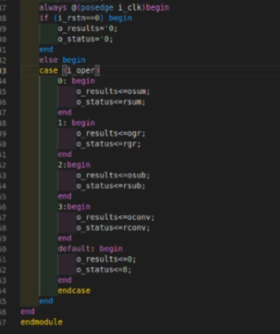
dziwny_mux.png

It looks like as if the multiplexer (which is this "case" here) is something like synchronized mux like here:
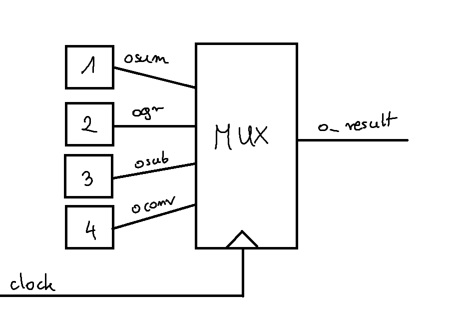
obraz_2022-12-06_002042887.png

Something like that exist ? I couldn't find something like that on the website.

But my code looks a bit different more logical
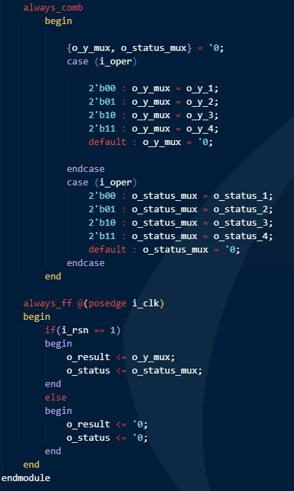
obraz_2022-12-06_002145294.png

It has 2 multiplexers and 1 flip-flop (this flip-flop is in always_ff)
So it looks like that :
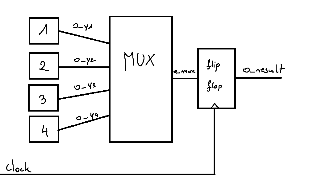
obraz_2022-12-06_002440357.png

sorry for this stupid question. I just don't know how the yosys will create a multiplexer with a clock input, when I couldn't find anywhere in the internet any schematics on how it looks like. In other words I don't know how to create mux that is synchronized without additional flip-flop on the output.
Because I only found typical multiplexer without clock, but this code says that the multiplexer has a clock. How to make multiplexer with clock ?
 

First of all, don't post a crummy, out of focus screenshot if you expect anybody to look at your code.

Second of all, your self-proclaimed "logical" code does not have one flip-flop, it has two.

Thirdly, the original code will just infer flip-flops where required.
 

First of all, don't post a crummy, out of focus screenshot if you expect anybody to look at your code.

Second of all, your self-proclaimed "logical" code does not have one flip-flop, it has two.

Thirdly, the original code will just infer flip-flops where required.
Sorry for the code from the first screen shot. I was doing it in a hurry.
About the flip-flop yes it has two flip-flops but the idea itself was to transfer data from mux to flip-flop and that's how I have understood the program will do.
So I don't really know how the program understand that the mux is in always_ff. It's like the flip-flop is also a mux. Like two modules in one module. I just couldn't find on the website any mux that has a clock like flip-flops have. So I couldn't imagine how the programs makes flip-flop multiplexer. I know it sounds wierd.
 

Both codes are exactly functional equivalent and resulting in the same FPGA implementation. The version with separate combinational and registered always blocks is in my opinion a lower level, longer winded and less readable coding style. If you sketch the logic as a circuit, I would nevertheless draw separated registers.
 

Both codes are exactly functional equivalent and resulting in the same FPGA implementation. The version with separate combinational and registered always blocks is in my opinion a lower level, longer winded and less readable coding style. If you sketch the logic as a circuit, I would nevertheless draw separated registers.
So how should I draw the first code with multiplexer and flip-flop in one ?
Or is it possible to make mux + flip_flop in one. Because I thought that maybe by drawing the circuits I could understand how the program will make the syntezis/make logic gate combination.
Because I don't know why but it buggs me off that the flip-flop is written as one module with multiplexer. Because I couldn't find a logic gates combination that shows it can be made. So I can't imagine how it looks like.
 

I think it's a misunderstanding. Clocking a module with blocking assignments means that the final ouput is registered. The preceeding logic is still combinational and not different from a purely combinational always(@) module.
 

The always_ff uses non blocking assignments (I don't really know what is the difference in blocking and non blocking).
But my main problem was purelly how the program understands it. Does it understand as making a mux with clocking or does it understand that he must make mux and connect it's output into input of an flip_flop with clocking ?
But this code looks like that mux with clock. And I imagine it that there is a mux with clocking system that works in D flip_flop or any similar to that.
So even if the program interprets it as a 2 separate modules (mux and flip_flop separate). So maybe I imagined it wrongly. I imagined always_ff as a flip_flop module. So it looked like flip_flop and inside of a flip_flop is multiplexer. Which didn't make sense to me if it comes to making a logic gate circuit
 

I imagined always_ff as a flip_flop module. So it looked like flip_flop and inside of a flip_flop is multiplexer.
It's synthesized as one FF per assigned variable bit plus combinational logic determining the input to the FF. Ending up in two FF and the same logic as in the combinational always block.
 

Status
Not open for further replies.

Part and Inventory Search

Welcome to EDABoard.com

Sponsor

Back
Top