Continue to Site

Welcome to EDAboard.com

Welcome to our site! EDAboard.com is an international Electronics Discussion Forum focused on EDA software, circuits, schematics, books, theory, papers, asic, pld, 8051, DSP, Network, RF, Analog Design, PCB, Service Manuals... and a whole lot more! To participate you need to register. Registration is free. Click here to register now.

three pin connector IC decoupling and bypass capacitors intuition

yefj

Advanced Member level 4
Joined
Sep 12, 2019
Messages
1,195
Helped
1
Reputation
2
Reaction score
3
Trophy points
38
Activity points
7,217
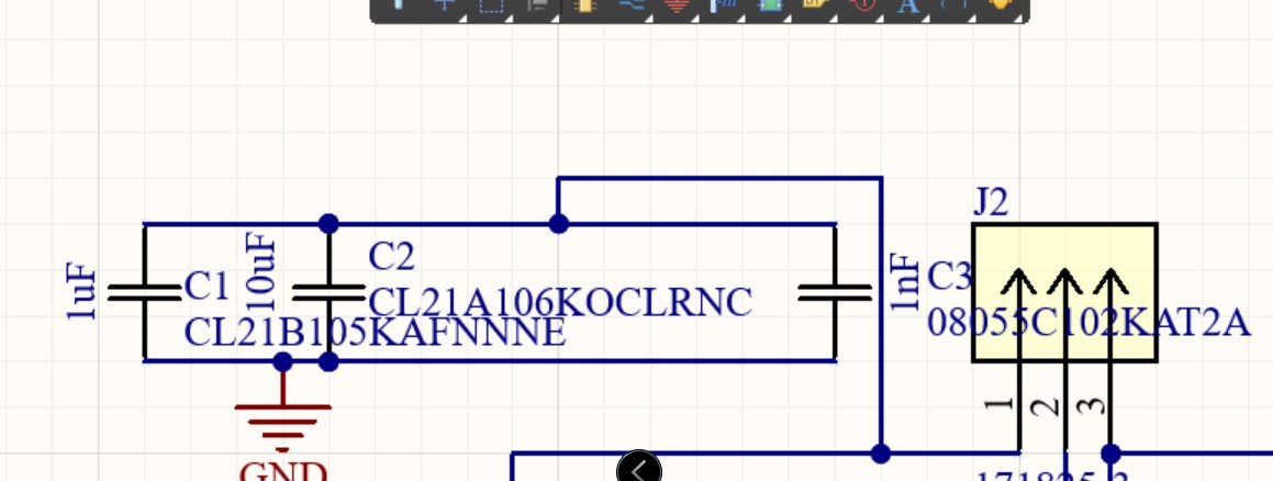
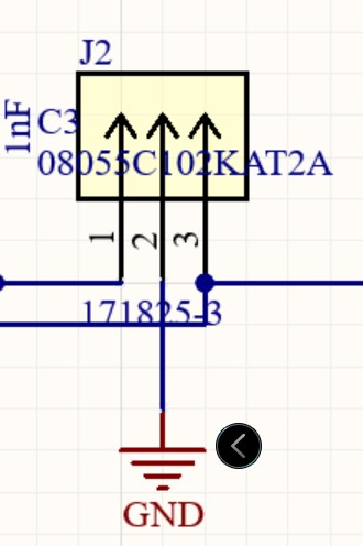
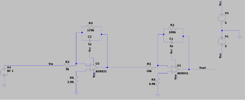
Hello, i have two issues when i build my circuit shown bellow:
1.regarding dec i have added decouplin capacitor as shown bellow but i am not sure if its betther to connect them on the side to the ground plane or its better to connect them between traces connected pins 1-2 and 2-3 ?

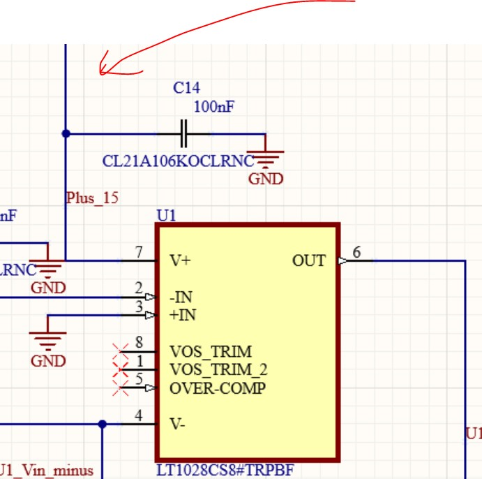
2.regarding bypass capacitors i have connected 0.1uF near IC to ground plane with a VIA as shown below.
Is it ok ? maybe i need to connect them as power rail between traces going straing from pins?
How do i know that 0.1uF fits my needs for bypass?
Thanks.
1697212556400.png


1697211973431.png
1697211823664.png
1697211798779.png
 
Look at it like this:

The entire purpose of the "decoupling" or "bypass" caps is to make an
AC short from supply to supply, such that any abrupt current event is
returned to the chip and does not escape to bother the neighbors -
while also providing close-in "make-up" charge. It's all, all about the
current / charge loop and the internal demand.

If you decouple V+ to ground plane and V- to ground plane, but
the "event current" runs from V- to V+, your decoupling will be
half as effective for the same C overall - series C, where it counts.

In multi-rail assemblies there may be more than one need. For
example maybe you have both a super abrupt internal switching
impulse per cycle, and a ground returned driven load. In that
case you may want both a very low ESR/ESL right across the pins
(for keeping internal supply rails stiff in-the-moment) and big
"reservoir" caps to whichever rails matter to the output (could
be V+ / Gnd, could be V+ / V-, could be V- / Gnd, depending on
the function, some or all). Like 10X the driven load capacitance
if you want "only" 10% supply droop at switching transitions.

You want to minimize "loop area" (for overall inductance, likely
to dwarf internal capacitor ESL) and pretend that the supply feed
is so inductive, that any switching energy must be provided by
the capacitors (@pin sum of internal and load).

If your chip design is fully represented then with realistic cap
component models you can do explicit design-for-power-
integrity with some confidence. But that representing, especially
board and package level parasitics can be a chore, the closer you
look.
 
  • Analog IC loads tend to be more constant and low dI/dt
  • Yet they are more sensitive to poor PSRR at higher frequency.
  • But large caps like 0.1 uF are limited by their self-resonant frequency.
  • If you are using HF then consider small values near the analog load. like 10 nF which is 1 Ohm ~ 13 MHz.
  • With mixed logic, analog and switched power, consider what is used in your voltage source. SMPS or Linear?
  • For SMPS there can be a risk of choosing the wrong caps that resonate with harmonics of the switching rate > 1MHz.
  • Bigger caps also have larger ESR and longer parts add ESL >~0.5nH/mm but vary with materials
  • The DC load error depends on the ratio of source to load resistance.
  • The bulk of the AC noise error depends on decoupling as much as possible at the offending dI/dt load. Such as logic circuits and uC which are essentially switched capacitors with a small Rs for dynamic dissipation.
  • The choice of decoupling thus depends on how much logic and switched inductive noise is on the rails or if SMPS ripple must be rejected.
  • You want to avoid sharing switched power paths with analog power and ground paths, so you label them separately, Agnd Dgnd or Pgnd in case this high-frequency glitch is not rejected by either the linear IC PSRR or the power RLC response curve.
  • Adding caps with awareness of trace inductance (ESL) and RLC resonance comes with experience and gets easier to understand with a simulation.
In the old days, we just used 3 values to spread out the upper limits like 1nF, 100nF, 10 uF when we had no idea what the noise would be. But now SMPS can be a problem as well as switched inductive loads.

When it's critical, add test points for Vcc and Gnd about 4 mm apart for use with a 10:1 probe with no clips just tip & ring with a gnd spring adapter.

With this nomograph , one can read Q, gain, loss, breakpoint or choose any of the 4 variables. We had paper sheets in the 70's with this.
1697217066653.png

--- Updated ---

For example if you have any noise at 3MHz on your supply here it will be amplified by 31 dB.

30 nH represents ~ 2~3 cm path length for power + gnd and using an ideal 0.1 uF cap.
1697219251293.png
 
Last edited:
Hi,

a schematic shows which pin from which device is connected to the pin of another device.
It does not show any physical placement.
But physical placement is important for the proper function of the decoupling capacitors.
Also all the wiring with the resulting series impedance.
Thus we need to see the PCB layout.

In post#1 you talk about a connecteor. But a connector itself is the least critical device regarding power supply decoupling.
It may be long cabling that receives or sends out noise. In this case we need to see a photo of the cabling with all it´s length and eventually noise sources nearby. This may be a reson for capacitors close to connectors.
While it follows about same rules as power supply decoupling, this more applies to EMI/EMC problems and the according capacitors.

You need to install the decoupling capacitor close "to the source of noise".
The source of noise
* may be a potentially ringing linear voltage regulator
* for sure is the output of a switching regulator
* is the power supply af a digital IC
* a fast OPAMP (drawing AC current from the power supply line)
...

Klaus
 
Hello Klauss,My implementation of the circuit is shown in the photos below.
From the internet i found these advices. i put 0.1u betwen IC +15 and gnd for every IC.
but then they say " Route PWR through the capacitor pad to force the flow between the source and ICs"
i cant emagine these words.
what is the meaning of forcing the flow between the source and IC?
is there some visual i could see the meaning of this advice?
Thanks.


"
Bypass caps need to be as close as possible to the power pin of each IC and power sources. Ideally they should be placed before most other routing so appropriate area is designated. Route PWR through the capacitor pad to force the flow between the source and ICs. Be sure to verify GND path of bypass caps are short routing back to IC GND pins/GND copper on bottom side.
Top side copper can be poured GND and/or PWR rails depending on current requirements."

1697310225110.png


1697310130826.png
 

LaTeX Commands Quick-Menu:

Similar threads

Part and Inventory Search

Welcome to EDABoard.com

Sponsor

Back
Top