Continue to Site

Welcome to EDAboard.com

Welcome to our site! EDAboard.com is an international Electronics Discussion Forum focused on EDA software, circuits, schematics, books, theory, papers, asic, pld, 8051, DSP, Network, RF, Analog Design, PCB, Service Manuals... and a whole lot more! To participate you need to register. Registration is free. Click here to register now.

three noise maker, but different output offset

canlu

Newbie level 6
Joined
Feb 4, 2024
Messages
12
Helped
0
Reputation
0
Reaction score
0
Trophy points
1
Activity points
76
hi.
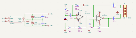
i have this circuit with op37 op-amp, and repeated three time.
media-1196822-di5436fig1s.jpg

but at output i have different offset according to pictures:
s1 .jpg
s2.jpg
s3.jpg

every thig is same and resistor's are 1%.
even in the output i have mkt cap.
what can cause such behavier in this circuit?
 
Where are you scoping the three signals and under what conditions?
What supply voltages (VCC and VEE) are you using to the ICs?
@room tempratore +- 15V
non-isolated osiloscope and three circuit Isolated By MinMax DC-DC (MAU327) and without x-cap
 
it's the real schematic, and yes d1 has same GND as R2
oscop connect between GND and pin2 of J1
thank for replay :)
 

Attachments

  • realSCH.png
    realSCH.png
    44.2 KB · Views: 60
Additional problem, large DC output offset of 2nd stage due to 11k overall DC gain, therefore asymmetrical clipping. 1st stage input offset is dominated by input bias current voltage drop. OP 37 isn't well suited for large source resistance. You want to use AC coupling between stages and FET amplifier for 1st stage.
 
secound amplifire isn't important. secound stage is not placed...!
how it would be different offset after C1(MKT)
 
These Op Amps have a high bias current (compared to 1pA FET input buffered types) your design which has mismatched high 1Meg and 1k source resistors with a gain of 11k which can produce an offset.
1707247430900.png

Also you may want to unclip the white noise to avoid introducing harmonic distortion.

- pin 1 is normal clipping +/-15V with measurement errors on DSO with capacitor charge.

1707244963495.png


Try showing J1-3 from U0-6 (haha BCD encoded RefDef)
 
Last edited:
I received the circuit today.In the reviews,
I saw that there is an offset at the displayed point.
op-amp input offset.png

What causes the offset at this point?
(capacitor's is MKT)
and even after c1 i have offset :(
Does the capacitor not eliminate DC?
 
What is value off offset you read ? Max Ibias x 1Mohm to ground = Voffset = 35 nA x 1,000,000 ohms = 35 mV.

If you disconnect C4 what offset do you read ?


Regards, Dana.
 
What is the result of reducing gain?
You have two different schematics
#1 has 2 stages each x10 with DC coupled outputs.
then you show another schematic with 1st stage with 1Meg and 60 dB gain with saturation almost 30Vpp and AC couple with large caps that with a single shot capture can show a DC offset due to the cap not being discharge to 0V

So reducing the gain is necessary to prevent clipping then let the output settle to 0Vdc after several time constants.RC=T if you want to AC couple.
So your 3 different results have undefined capture conditions. What are all the assumptions we should know?
OK?
 
i'm now understand. thank's
D2 is 9.4V Zener So by removing C4 input offset Would be 9.4V
i'll change R4 Value and Measure Value's..
@D.A.(Tony)Stewart
l Measure value and inform theme
thank's so much🙂
 
Last edited:
i'm now understand. thank's
D2 is 9.4V Zener So by removing C4 input offset Would be 9.4V
i'll change R4 Value and Measure Value's..
@D.A.(Tony)Stewart
l Measure value and inform theme
thank's so much🙂
No do not remove C4
 
i have -116mV, + 267mV signal there.
decreasing R17 to 500k not affect.
i'll test decreasing R4 tonight.
op-amp input offset.png
 
The OP37 Ibias is a max of 40 nA, so a change from 1M to 500 K
would only change the Voffset due to Ibias from 40 mV to 20 mV.
worst case. So that would be x gain to find the output. The typical
offset is 10 nA so that would be much less.

So Vout = 1001 x 20 mV ~= 20V which would sat the OpAmp output.

Either drop G or get OpAmp with much less Ibias. Or add offset adjust
circuit :


Regards, Dana.
 
Last edited:

LaTeX Commands Quick-Menu:

Similar threads

Part and Inventory Search

Welcome to EDABoard.com

Sponsor

Back
Top