Welcome to our site! EDAboard.com is an international Electronics Discussion Forum focused on EDA software, circuits, schematics, books, theory, papers, asic, pld, 8051, DSP, Network, RF, Analog Design, PCB, Service Manuals... and a whole lot more! To participate you need to register. Registration is free. Click here to register now.
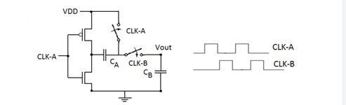
Draw the output waveform Vout for the circuit shown below against time for a clock cycle of 5. Consider the Switches are Ideal and CA is equal to CB. (Ignore the Parasitic capacitance)
The upper transistor is P type.
The bottom transistor is N.
Current goes through capacitor CA first in one direction, then the other.
Do the above hints suggest what happens at the output? It may be unexpected since this circuit is seldom seen yet it's a useful building block circuit.
This site uses cookies to help personalise content, tailor your experience and to keep you logged in if you register.
By continuing to use this site, you are consenting to our use of cookies.