Continue to Site

Welcome to EDAboard.com

Welcome to our site! EDAboard.com is an international Electronics Discussion Forum focused on EDA software, circuits, schematics, books, theory, papers, asic, pld, 8051, DSP, Network, RF, Analog Design, PCB, Service Manuals... and a whole lot more! To participate you need to register. Registration is free. Click here to register now.

Supply voltage disturbance in mixed-signal IC

Status
Not open for further replies.

Junus2012

Advanced Member level 5
Joined
Jan 9, 2012
Messages
1,552
Helped
47
Reputation
98
Reaction score
53
Trophy points
1,328
Location
Italy
Activity points
15,235
Hello friends

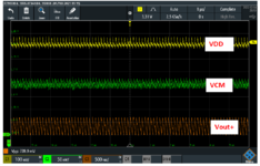
I have practical issue after received our chip prototype from foundry, the alternative drop in the supply voltage due to the switching activity of the digital clocked circuits in our chip,

I admit that supply line disturbance is expected practically due to switching currents that develop a voltage drop on the supply output resistance. However, I am using LAB supply voltage where I am surprised to see him suffer like this, it is not simple LDO circuit !!

What I need to conclude, using an ideal voltage source is not the right when simulating Mixed-signal IC with Cadence (or any other type of simulation), for example, I have the same simulation setup of the measurement and I see that switching activity has zero effect on the supply voltage (ideal voltage source) in my simulation results.

Since I want to learn from my practical results and to make a more realistic simulation with Cadence in the future, I would ask for you suggestion for using the ideal voltage supply in the circuit simulation, like do I need to connect a small resistor in series to represent the output resistance. What else I can consider to make the switching effect predicted by simulation.

Thank you in advance for your help

Best Regards
 

Modeling bond wires as 1nH and 0.1 ohm is a reasonable first stab. But if this at die probe you can expect more like ohms or tens of ohms from probe and contact resistance.

If you believe this is a dynamic problem more than I_average*R and you are in a package already, consider "tombstoning" a capacitor on the cavity floor, down bond as many grounds as you can and skip-bond the Vdd across the top of the cap on the way from pad to post.

You might look at activity right before the "WTF?!?" To see if there is consistency in things like a vector where all the outputs switch simultaneously? Also you can cut the impact of this by not putting canonical 50pF (or whatever) loads on every logic output, removing loads and probes from anything you are not presently looking at, even putting series R between outputs and their load & harness.
.
 
Last edited:
Lab Power Supplies have normally very low internal impedances and they can easily be considered as almost Ideal.
But if you have been used "cheapo" supply, a transient voltage drop may occur. Connect a electrolytic capacitor near to chip to prevent instantaneous voltage drops.
Or replace the power supply with a high quality one.
 
In addition to all good advices above - I would suggest to check or to do the following:

1. Use different ground / power nets for digital and for analog portions of your design (if possible).

2. If (1) is impossible - try to connect digital and analog portions of ground and power nets right at the ball/pad, to minimize common resistance for analog and digital blocks.

3. Check (simulate/analyze) the resistance of the power/ground nets, and common resistance between analog and digital blocks.

4. Use decoupling capacitances.

The problem with power nets is that they can be large or humongous, so the size of the post-layout netlist, if you add power nets to extraction, can be huge, and hence simulation can be very slow.

That's why industry is using power net analysis tools (such as Totem, Redhawk, Voltus / VoltusFi, ParagonX / PrimeX, etc.) to simulate them faster, more efficiently.
 
Dear friends,

Thank you very much for your discussion,

I want to tell you that Our package type is PGA 100 (Ceramic Pin Grid Array), one thing might be useful to mention, our chip area is small as compared to the package cavity but we used this type of package because we need 100 pins. As a consequence, the bonding wires are were to the maximum length allowed for packaging.

Actually, the bonding wires was not considered by our simulation with its inductance, capacitance and resistance effect that also give an answer to the difference between out simulation in Cadence and the practical measurements we are observing. The highest level of simulation we performed is by including the pad frame. Even we are not aware if there is a simulation possibility that includes the package/bonding leads effect and could be interesting to know.

I would like to share with you a snap screen from the oscilloscope measurement of the fully differential amplifier circuit. In this setup the amplifier both inputs are tied to the mild supply voltage, the same for the common mode voltage of 1.65 V where we use VDD=3.3 V.

Ideally the differential outputs should be equal to VCM= 1.65 V as also proved by simulation, in addition to differential offset, however we set the closed loop gain to unity so th offset voltage should not be effective.

When you look to the output you see the noise coupled at one of the outputs, Vout+ and also the noise coupled to VCM and VDD rails. Note that VDD and VCM are both provided directly from the power supply.

I believe that noise should be random but what we see is deterministic noise looks like oscillation. On the other hand, we could use the ircuit to amplify by varying the gain level and also the SNR becomes better with higher signal amplitude, which means that if the circuit is still working as a linear amplifier cause if the circuit is not stable/oscillating it can not be used linearly.

I am apologizing if I made the post lengthy and thank you once again for your kind help

Regads
 

Attachments

  • noise.PNG
    noise.PNG
    108.9 KB · Views: 111

you got problems - possibly not enough gnd wires and Vcc wires in your 100 pin design - minimum one pair per side ( 8 wires total ) to allow caps to keep these rails stiff, at high speed long bond wires can easily contribute to instability and quite possibly oscillation, and poor coupling of power supply caps to the IC itself ...
 
Worth noting as well, that basic area-array packages tend to use fine, long, undoped tungsten conductors in the fired body and the internal trace resistance and inductance will far exceed the bond wire. These traces are also highly variable, with the ones from post-ring to center being quite long while ones right below the bond shelf will be minimal(ish).

In Spin2 you might drill into this with the package vendor, select lowest-impedance pins for power and grounds, fill any empty posts with cavity down-bonds and pick up all vss from cavity floor, etc.

I'd have to set the Wayback Machine to 2005 or so, to dig up info on internal trace materials/electricals but if it's useful I can. You might find info faster by other avenues.
 
Dear friends,

I am very grateful for your help and the valuable comments you advised me to do,

I would like to give you a feedback on it, rather we made new PCBs and located the capacitors near to the VDD, GND pins. We optimized the power routing as well with PCB ground plate. As a result the noise is largely reduced.

However, the reality behind the large amplitude of the signal I shared before was in a noise, we dicovered that our amplifier was not too much stable and those are oscillating signals.


Back to the noise improvement, we have foundout new thing that might be another reason for noise contribution, during the design package, we did not connect the chip substrate to the package cavity. In some design I have explored, I found that people are using epoxy conductive glue to attach the die to the package cavity then they routed to a ground pin or sometimes to the available extra pin of the package. So we have unfortunately missed this, and I would like to ask from your experience how big is important this step.


Thank you
Best Regards
 
The substrate (if JI) would have some ohmic access
through the negative pads but this will also have some
significant inductance. This could be a "special tank".
But this could easily be messed with in a custom bond
figure, adding down-bonds and up-bonds to tighten it
up.

SOI, you have to down-bond to get control of that floating
node.

You can usually get 2-4 bond wires per post in older
ceramic packaging, which people still use for prototyping
if the production target package is of similar mechanical
outline. I'm not hep to that small-outline leadframe
jive, though. Point being maybe you don't need to find an
uncommitted pin, just place bond roots where there's
room remaining on the post finger.
 

    Junus2012

    Points: 2
    Helpful Answer Positive Rating
Aaah...

" However, the reality behind the large amplitude of the signal I shared before was in a noise, we discovered that our amplifier was not too much stable and those are oscillating signals. "

It certainly looked like that for the Vout signal shown above.
 
Status
Not open for further replies.

Part and Inventory Search

Welcome to EDABoard.com

Sponsor

Back
Top