Continue to Site

Welcome to EDAboard.com

Welcome to our site! EDAboard.com is an international Electronics Discussion Forum focused on EDA software, circuits, schematics, books, theory, papers, asic, pld, 8051, DSP, Network, RF, Analog Design, PCB, Service Manuals... and a whole lot more! To participate you need to register. Registration is free. Click here to register now.

Substrate definition of transformer

Status
Not open for further replies.

Manjularamkumar

Member level 1
Joined
Aug 16, 2011
Messages
34
Helped
0
Reputation
0
Reaction score
0
Trophy points
1,286
Activity points
1,507
Hi ,

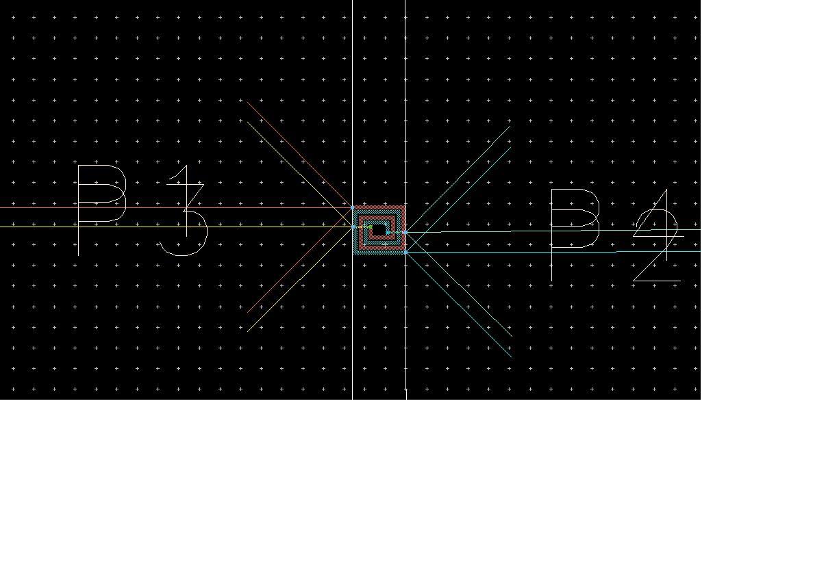
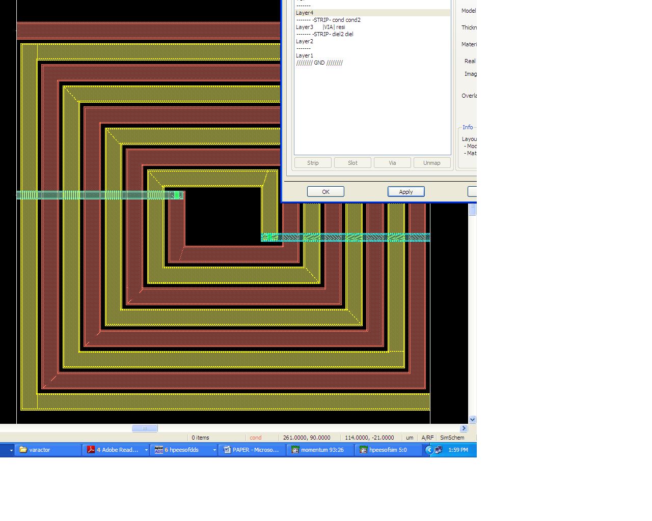
I am designing transformer. I follow the substrate definition of inductor on silicon

Top
-------- Strip -cond2
layer3 Via |resi|
-------- Strip cond
Layer2
---------
Layer1
//////GND//////

For transformer design , I have to use two different metal lines
Top
-------- Strip -cond2 cond
layer2 Via |resi| |hole|
-------- Strip diel2 diel
Layer1
//////GND/////

Is it correct sir? T I hereby attached the example design. Please see and tell your suggestion for transformer design.Please help me .


Urgent
 

What is your top? Air? I think you should add some substrate above cond2. I can't see your example. Software is ADS momentum?. Your stack-up for transformer design: Why you use two layers (resi and hole) for via definition?

Maybe some example:

Top [AIR]
subst
-------- Strip
subst Via
-------- Strip
subst
---------
Si
//////GND//////
 

Hi,

Thanks. Now I used one layer for via and two layers for metals and underpasses.See my design


Maybe post again your stack-up because a layer for vias seems not to be correct, it should be inside the substrate layer.
 

Hi,

I couldnt understand. I think , i incorporate your comments. Please see my design . Where i made wrong? Please correct it.


Maybe post again your stack-up because a layer for vias seems not to be correct, it should be inside the substrate layer.
 

Hi, What is the purpose of take layer 1 and layer 4 here?? Is it to confine the fields around the inductor structure??
 

I dont know. I have seen some examples in ADS so I put.

Yes u r correct. Ill remove layer 1 and 4. Otherwise the design is ok.


Hi, What is the purpose of take layer 1 and layer 4 here?? Is it to confine the fields around the inductor structure??
 

Is it a transformer that u r trying to simulate or just an inductor?? Clearly the structure is an spiral inductor, and Planar transformers are totally different having cores and etc.. ?
 

i am trying mutual coupled inductors . Please explain where it is wrong?


Is it a transformer that u r trying to simulate or just an inductor?? Clearly the structure is an spiral inductor, and Planar transformers are totally different having cores and etc.. ?
 

Status
Not open for further replies.

Part and Inventory Search

Welcome to EDABoard.com

Sponsor

Back
Top