Continue to Site

Welcome to EDAboard.com

Welcome to our site! EDAboard.com is an international Electronics Discussion Forum focused on EDA software, circuits, schematics, books, theory, papers, asic, pld, 8051, DSP, Network, RF, Analog Design, PCB, Service Manuals... and a whole lot more! To participate you need to register. Registration is free. Click here to register now.

strategy for designing a locking component in PLL

yefj

Advanced Member level 4
Joined
Sep 12, 2019
Messages
1,196
Helped
1
Reputation
2
Reaction score
3
Trophy points
38
Activity points
7,223
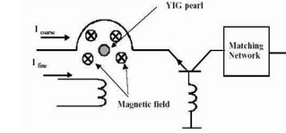
Hello,there is a circuit shown below taken from the attached article, where we put a YIG signal to a cavity resonator(from A to B) .
Then for feedback we lock on the point of the dip.
this dip is supposed to be a resonance of a cavity.

resonance is when the magnetic energy equals the electric energy maximal energ is stored in the cavity.
So why for feedback we lock on the cavity at this point?
Thanks.

1689653829043.png
 

Attachments

  • High_spectral_purity_microwave_oscillator_design_using_conventional_air-dielectric_cavity.pdf
    563.8 KB · Views: 77
Hello,I have a feedback loop as shown below,We are fixing the noisy YIG with a cavity resonator and feedback.(shown in the attached paper and diagram below).
the phase difference between the signal is transformed into voltage that feeds the yig and changes the frequency of the YIG proportionaly with the voltage we enter.
generally speaking if i use a amplifier as shown bellow then from control theory i get P controller.
1.What if i want to create a PID controller for the error fixing,will it work better?
could you please reccomend me tip on how to make a good PID that will .
from the diagram beloow i have thee components.how do i know how to plan the PID properly for my system it has coefficients.
how do i deside what K_P K_I and K_D to create?
Thanks.
1695392568374.png


1695393083702.png
 

Attachments

  • High_spectral_purity_microwave_oscillator_design_using_conventional_air-dielectric_cavity.pdf
    563.8 KB · Views: 57
Hello, i am trying to implement the circuit shown bellow.its a PLL device.the mixer produses DC voltage signal which is error between the reference oscilator and the main oscilator as described in the attached article.idially the error voltage needs to be zero and the reference frequency needs to match the main oscilator frequency.
basickly the heart of it is the SERVO amplifyer.the servo amplifyer takes the error voltage and converts it into chaging the reference oscilation of frequency.
looking at the diagram bellow is there a way to predict wether servo amplifyer could achieve the desired locking between the refrence and main oscilators?
Thanks.
1702930340854.png
 

Attachments

  • High_spectral_purity_microwave_oscillator_design_using_conventional_air-dielectric_cavity.pdf
    563.8 KB · Views: 55
Hello Tony, In reality there is a YIG device changes its output frequency by the amount of voltage it gets from the servo amplfier.
The Yig signal get compared to the main oscilator signal using the mixer.

if we look into general control theory we see that we need to track the desired signal and eventually get the error voltage to reduce.
I can make a transfer function of them amplifier.
I also can try and do a table of by how much my YIG changes its frequency as a function of voltage.
Also i can record the initial error voltage between the YIG and the main oscillator.
but how can i combine them and see if my SERVO amplifier can do the job and succeed in making a lock of the YIG oscillator and main oscillator?
Thanks.
1702981767619.png


1702982095476.png
 
Ideal with any servo, use first order feedback for phase and frequency and 2nd order equation with type 3 compensator or type 2. Design specs must choose between jitter and capture range, lock-in time , may use dual bandwidth for fast capture, slow tracking.
The Yig is quite microphonic, so rigid ceramic construction with isolation is needed.

 
Hello Tony ,my problem is more of linking the real life to the theory.as you can see in the article and the photo from it.
The main oscillator is a resonator it produces an RF signal at one frequency.
the error voltage is voltage is a function of the difference between the YIG frequency and the main constant resonator frequency.
So regarding the YIG i can do a sweep of voltage to see the frequency response in the spectrum analyzer.
my main oscillator is a constant voltage.

my problem is linking the real life devices to the simulation i am trying to build.
i can sweep at the probable voltage range and see the error voltage which comes out from the mixer.

the servo amplifier (gets the error voltage) makes the YIG move by some frequency.
how can i take this real life extracted responses and see if my servo will do the job.
Thanks.
1702988779132.png
 
Bode & Nyquist Plots help define gain/phase margin. The partial differentiator in the type III compensator does this. It is chosen just before unity gain to provide phase lead compensation. Servo loop gain may be define by the spectral response of Kd, Ki, Kp but I prefer to use Bode Plots. The ideal filter is a tradeoff to meet all requirements for Lock-in range, lock-in time, and jitter reduction.

You want a minimum of 45 deg. Rise times BW-3dB~ 0.5/Tau (63%)

Plot for filter response and compare with error frequency. You need sufficient BW to capture the error with good phase margin. So the goal is to minimize your error frequency 1st.
 
Last edited:
the mixer in your system is acting like a DC coupled phase detector.
at resonance, the reflection coefficient angle of the Q=59000 resonator is ZERO degrees.
a little below the resonant frequency, the reflection coefficient is some number X. and the same amount frequency ABOVEr the resonant frequency, the reflection coefficien is -X. so the dc coupled mixer output puts out a + or - DC voltage depending on if you are just slightly above or below the resonant frequency.

That is the analog control loop you are trying to optimize, and make stable.
In addition, you have a carrier nulling section that removes the carrier and only lets the noise sidebands come out of the mixer output. So it will not be so simple to tune the yig oscillator until the mixer output is Zero Volts DC, since there is no carrier to generate the null!

Also, the YIG tuning coil has a LOT of gain to it (MHz/milliamp). This makes the system want to oscillate, since the open loop control gain is huge.

good luck

If i were you, i would get it all to work well without the carrier nulling loop attached. And then add the carrier nulling in later on.
 
Hello biff44,i have some question to better understand your explanantion:
1.the main oscillator gets a signal from the YIG .The oscillator sends back a signal with an amplitude depending on the oscillator resonance.
regarding what you say about the "angle" below.by angle i understand that the phase also changes when we move away from the resonant frequency?
Why do you say that the phase of the reflected signal will change?
" the reflection coefficient angle of the Q=59000 resonator is ZERO degrees."

2.So what is the logic of putting this carrier nulling section if need to compare the YIG RF signal with the main oscillator RF signal?
"carrier nulling section that removes the carrier and only lets the noise sidebands come out of the mixer output So it will not be so simple to tune the yig oscillator until the mixer output is Zero Volts DC, since there is no carrier to generate the null!


3.regarding the servo amplifier how do you propose me to check in my lab the my servo amplifier will succeed in doing the locking.
i can record the signal coming out of each device. also i can create a transfer function
how do you propose me to convert this recorded data into a simulation?

1703055124920.png
 
You are trying to implement an analog PLL. The servo amplifier should accept error voltages at the output of the mixer, it requires a symmetric supply. Its ouput should be wide enough to cover the tuning voltage range of the YIG.

Have you worked on an analog PLL before? The first step should be a simple analog PLL, it is to lock the YIG to an external reference instead of the cavity stabilization. Start with P-control having high gain (say 100V/V or higher). You can build an active loop filter (servo amplifier) using the difference amplifier topology. The amplifier should accept externally applied bias voltage so that you can set the output DC voltage to tune the YIG, the difference amplifier topology allows controling output DC. Once you construct the setup, inject the external reference at a frequency close to the frequency generated by the YIG, they should be (quadrature) locked. You can perform analog PLL simulations in Mathworks Simulink.
 
Last edited:
Hello Ferdem, i have all the devices.
how can i convert them into matlab simulink?
also if you could please give an opinion regarding the questions in post #10?
Thanks.
 
Why do you say that the phase of the reflected signal will change?
Reflected signal has a band-stop characteristic with respective phase.

2.So what is the logic of putting this carrier nulling section if need to compare the YIG RF signal with the main oscillator RF signal?
Circulator port c output has two unwanted carrier components due to
a. circulator leakage
b. resonator impedance mismatch
Its level is most likely higher than reflected signal minimum expected according to resonator Q. If not compensated, it would ruin phase detector operation.
 
If you do not know the transfer function of each component or can deal with the extreme high gain of varicap, then you might consider an easier more common method of tuning it with inductance using FLL and PLL with a scalers and a reference VCXO..

Generally, oscillators change the frequency by changing the capacitance. The YIG oscillator achieves this by changing the inductance. As the current through the coil changes, so does the magnetic field, and the inductance changes.

Then use a good simulator like Finesim or the one you know best to test your servo loop filter compensator for stability.


Attachments

  • 1703181598608.png
    1703181598608.png
    40.7 KB · Views: 40
Last edited:
Hello , i can view each point on the diagram using spectrum analyzer or osciloscope.
When i will connect the system how can i investigate in real life?
Is there a way to investigate the locking of a PLL?
Thanks.


1703250653002.png
 
FLL lock-in and PLL responses can be modeled in the time domain if parasitic environmental noise and carrier leakage is included to reduce SNR or the frequency domain with Bode plots with expected signals to analyze phase/gain margins. But note the assumptions are hard to model without real experience, which I have only read about.
 
i can view each point on the diagram using spectrum analyzer or osciloscope.
I guess you can't. You can't probe 10 GHz with an oscilloscope. There are only few circuit "points" that can be connected to a SA without affecting operation. For smallest impact, you'll e.g. use a coupler with high attenuation, -20 dB or more. Can be used to monitor oscillator output with SA.

PLL locking can be probably detected at the mixer and loop amplifier output.
 
Hello , i got to the conclusion that as you said before the YIG will look for the resonance point of the main resonator.
the point where S11 is the lowest.
So i will need to look at the output of main oscilator and see how it moves at some frequency band back and forth and at some point its amplitude power will be the highest.

regarding what biff44 said below:
why at resosnanse the phase of S11 is zero?
Thanks.

biff44:
"the mixer in your system is acting like a DC coupled phase detector.
at resonance, the reflection coefficient angle of the Q=59000 resonator is ZERO degrees.
a little below the resonant frequency, the reflection coefficient is some number X. and the same amount frequency ABOVEr the resonant frequency"
1703261566954.png
 
yes, that is correct. However, the balanced mixer is a phase detector as the formula shows but it’s limited in the range of phase so if you exceeded the phase error, it goes from negative feedback to positive feedback. Also, you have to get frequency loop FLL and as you know frequency is the derivative of phase. So in your PID compensation loop filter, you need a partial derivative as I explained before in order to have adequate phase margin for the error frequency in your loop gain
 

LaTeX Commands Quick-Menu:

Similar threads

Part and Inventory Search

Welcome to EDABoard.com

Sponsor

Back
Top