Continue to Site

Welcome to EDAboard.com

Welcome to our site! EDAboard.com is an international Electronics Discussion Forum focused on EDA software, circuits, schematics, books, theory, papers, asic, pld, 8051, DSP, Network, RF, Analog Design, PCB, Service Manuals... and a whole lot more! To participate you need to register. Registration is free. Click here to register now.

Splitting of Ground plane for Analog signals and DC supply

Status
Not open for further replies.
Hi vikash,
once complete the placement apply the copper in plane area (gnd and power ) and post the gnd and power layer in snapshot
 

Hi ,

I have attached the datasheet link of a ferrite bead. I need to use it in my circuit design for 24V input and can handle 500ma. Could you please tell me what is the relation between impedance and DC resistance. How do I need to select the ferrite bead in order to suppress the output noise with relation to impedance and DC resistance? Is low impedance and low DC resistance is a better ferrite bead or high impedance and high DC resistance is better ferrite bead ?

https://www.farnell.com/datasheets/5202.pdf

Thank you.
 

The more I read the more I realize that my complex mixed-signal design with a sensitive Analog Front-End will be hurt by split grounds.
However, I would like to confirm it here If it worth it or not to split the grounds.

planes.jpg

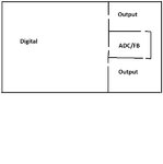
This is my internal ground plane on my 4-layer board. I will pour the ground planes on top and bottom copper layers as well and separate them in the same areas.
The 3 connections points between the digital ground and other grounds lay underneath mixed-signal ICs.
Overall, it looks like my analog and digital signal traces and the return paths are separated and do not cross the void copper of the ground planes. But my power rails, both analog and digital, cross the separation line between the grounds. I have seen some reference designs in AppNotes where power rails crossed the void copper lines. But, I am not sure if it is a good practice. I have 7 different supply rails for the output/feedback stage, so it is not possible to route without void copper area crossing a power trace/plane.
So, I have 3 options.
1. Split ground planes with power rails crossed by separation line (void copper).
2. The same as 1, but with jumpers on top and bottom to connect the ground planes if the system gets dirty, like Henry Otts suggested.
3. One ground plane for the whole board.

What do you think?
 

It is a hard question to answer, I do contract PCB design for numerous people and the variations of grounding schemes is vast, some would have one ground, some would split it like you do. Its a hard one to call without intimate knowledge of the schematic, parts etc.
 

Status
Not open for further replies.

Part and Inventory Search

Welcome to EDABoard.com

Sponsor

Back
Top