Continue to Site

Welcome to EDAboard.com

Welcome to our site! EDAboard.com is an international Electronics Discussion Forum focused on EDA software, circuits, schematics, books, theory, papers, asic, pld, 8051, DSP, Network, RF, Analog Design, PCB, Service Manuals... and a whole lot more! To participate you need to register. Registration is free. Click here to register now.

Snapback: when does a nmos EXIT snap behavior?

Status
Not open for further replies.

davestew

Junior Member level 1
Joined
Feb 5, 2012
Messages
17
Helped
0
Reputation
0
Reaction score
0
Trophy points
1,281
Activity points
1,459
Hello all,

I have a question regarding the snapback behaviors of a nmos transistor (used in esd protection).
I understand that the nmos will enter in snapback behavior when its drain will exceed Vt1 and pull back the drain voltage to ~Vhold depending on the current entering the drain.
However, what I am not sure of is when does the nmos transistor exit its snap behavior/s-shaped I-V characteristic and fall back in the normal operation I-V characteristic. Is it when the current being pushed into the drain drops below Ihold, where Ihold is the corresponding current to the Vhold on the s-shaped snapback I-V characterisitic?

Any help will be appreciated
Regards,
Dave
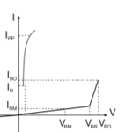
 

... Is it when the current being pushed into the drain drops below Ihold, where Ihold is the corresponding current to the Vhold on the s-shaped snapback I-V characterisitic?

Yes: it falls back from IH to the correspondent current point of the "forward" characteristic: trisil_characteristic.png
 

Thank for you reply erikl.
Clarification: By "forward characteristic" do you mean the saturation (region II) or triode (region I) regions of the I-V mosfet curve ?

-Dave
 

You cannot easily differentiate between these 2 regions for an ESD device (gate usually short-circuited to source) because - what I called "forward characteristic" - is a sub-sub-threshold I/V characteristic of a MOSFET, s. e.g. Fig. 2.6 of the PDF below. But I'd say the snap-back point IH/Vsb is more likely in the saturation region, as Vsb is still of the order of a few Volts.
View attachment CHARACTERIZATION,_MODELING,_AND_DESIGN_OF_ESD_PROTECTION_CIRCUITS.pdf
 

Thank you again for your reply and thanks for the document.

So basically, referring again to figure 2.6, when an esd event is finishing (i.e. esd current dropping towards 0A) the voltage on the pad will fall from Vh/Ih along more or less the IMAGINARY DASHED line and settle on the I-V part of the curve that lies BEFORE Vt1/It1 (i.e: the sub-sub saturation region) to a voltage ~Vsb. The dashed line is only there to indicate that the Vsb point is where the x-axis and the snap waveform linear portion (after Vh) would meet - it is not part of the snapback characteristic. The reason why I ask this question is because the s-shaped snapback waveform demonstrates clearly how the pad voltage will progress as the pad current increases but is unclear on how the pad voltage will behave when the esd current is falling. There is no second diode-like I-V waveform superimposed on the s-shaped snapback waveform showing that as the current drops the voltage will NOT go back to Vt1 and then drop to 0V but instead will take a different more direct path to the I-V origin.

Regards,
-Dave
 

Dave,

I think the I/V path from the left knee down to the Vsb point along the dashed line in fig. 2.6 (a) is due to voltage starving: the ESD source can't deliver a larger voltage any more to run back the "forward" snapback I/V curve which would need increasing voltage, but follows the 1/Rsb gradient down to the sub-subthreshold characteristic - and then back to zero.

Try and simulate the curve!

erikl
 

Status
Not open for further replies.

Part and Inventory Search

Welcome to EDABoard.com

Sponsor

Back
Top