Continue to Site

Welcome to EDAboard.com

Welcome to our site! EDAboard.com is an international Electronics Discussion Forum focused on EDA software, circuits, schematics, books, theory, papers, asic, pld, 8051, DSP, Network, RF, Analog Design, PCB, Service Manuals... and a whole lot more! To participate you need to register. Registration is free. Click here to register now.

Sinewave inverter prototype...

Status
Not open for further replies.
Final version of that AC220V 50Hz -> AC110V 60Hz converter.
 

Attachments

  • acac.zip
    6.4 KB · Views: 252

In post#204 looking at the ossiliscope signals the signals to the lower mosfets should be 50/60Hz to provide the return part to the upper mosfets, this is what i thought.

My other question is the pc817 based H-bridge driver can support 16khz.
 

at the ossiliscope signals the signals to the lower mosfets should be 50/60Hz to provide the return part to the upper mosfets
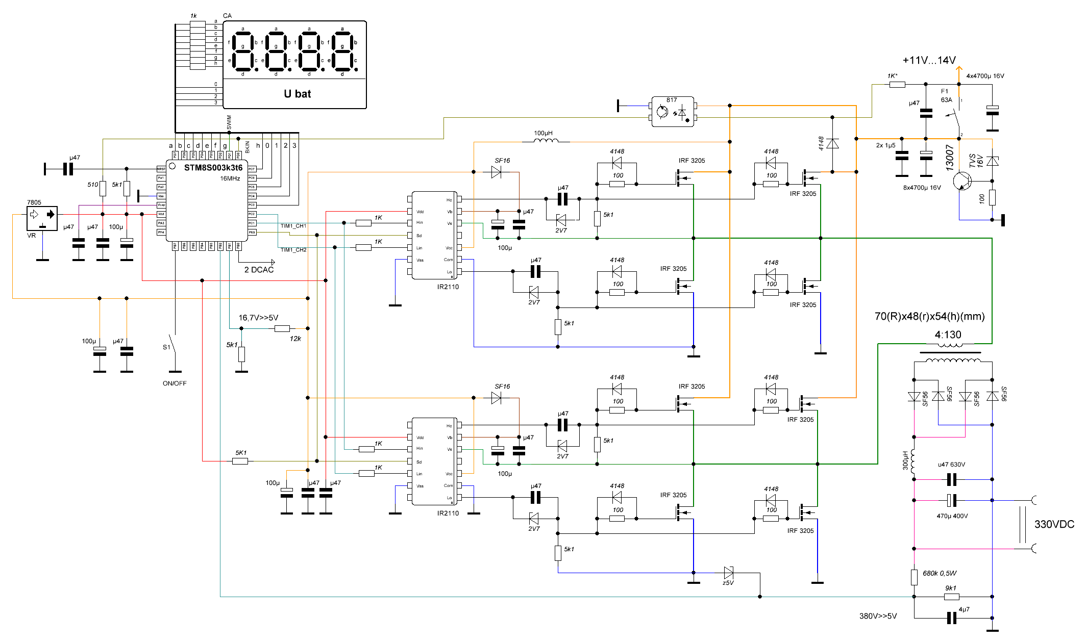
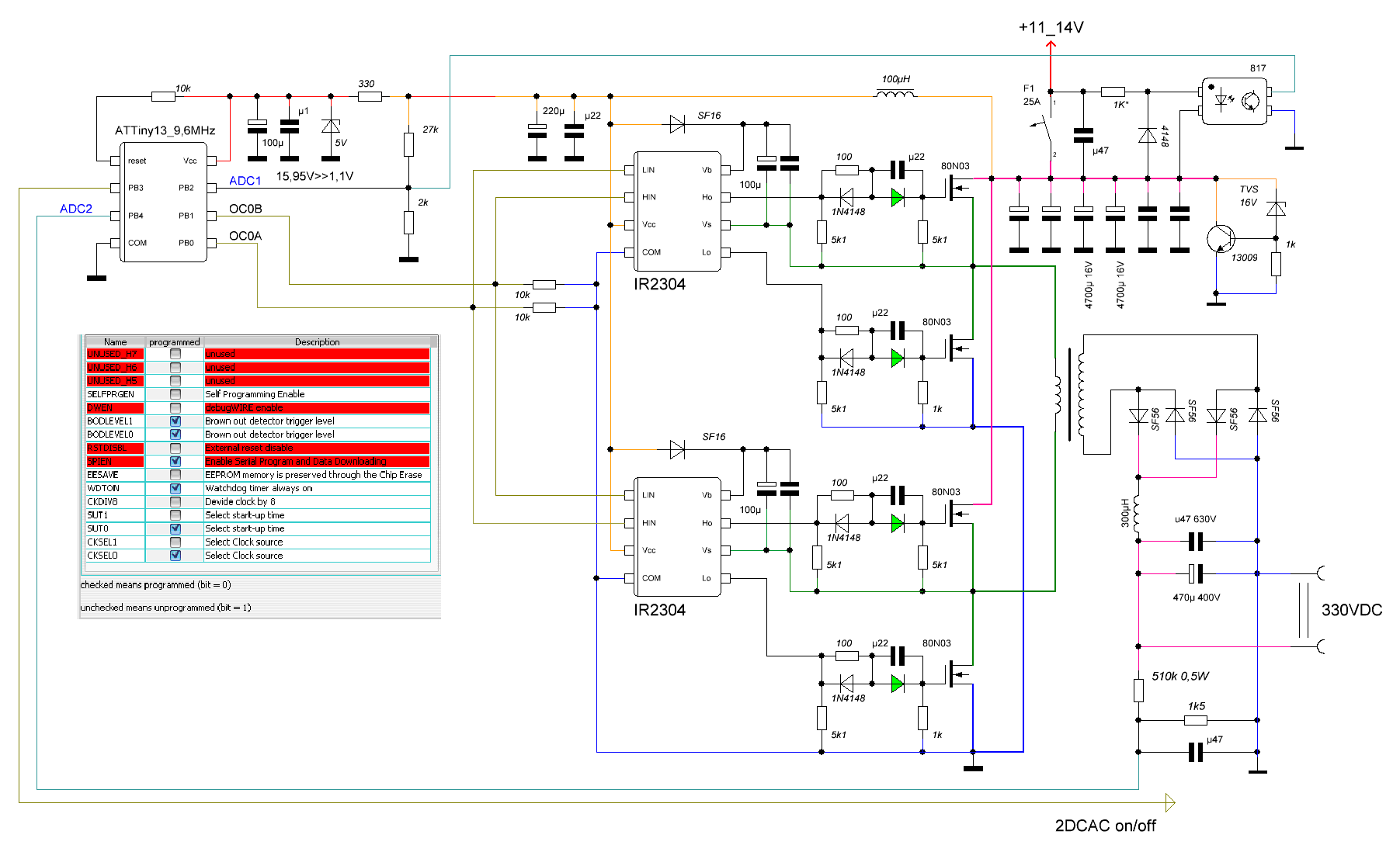
The osc signal low level for upper key corresponds to off condition, for lower key - on condition.
Thereby, the keys of one half of the bridge work alternately while other half has an switched off upper key and switched on lower key.
is the pc817 based H-bridge driver can support 16khz.
Response time of PC817 photocoupler is around 20us, so driver can support not more than few kHz.
__________________________________________________
next project - DC_DC 12>350V with increased power, sufficient for refrigerator with ACIM. Not ready in this time.


Ok I want to use this scheme for modified sine wave (square wave) for 50Hz, My question how you are driving the upper mosfets, in case if the frequency is 50 Not able to charge pump the capacitor.
will this driving stage able to drive 4-5 mosfets in parallal.
 
Last edited:

if the frequency is 50 Not able to charge pump the capacitor
Try to enlarge capacitor for charge pump, may be it will be work.
will this driving stage able to drive 4-5 mosfets in parallal
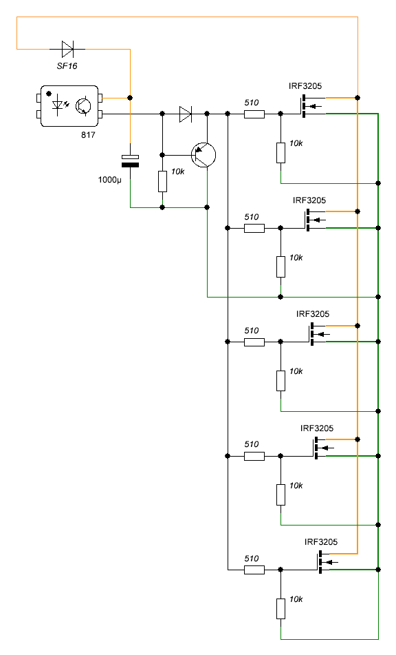
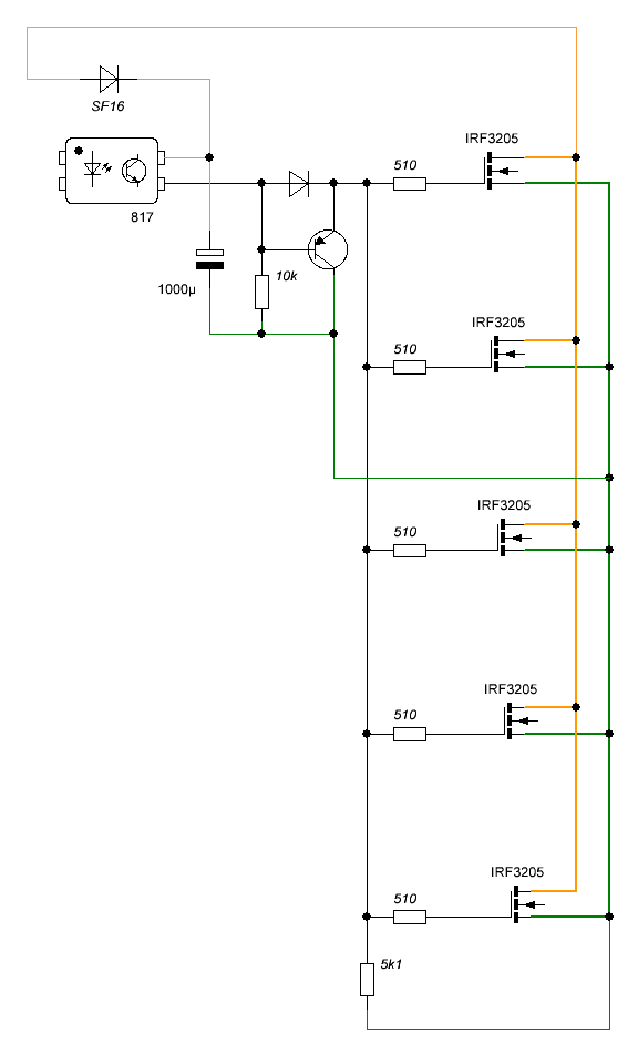
May be - if PC817<->gate resistors be increased to 510 Ohms and G_S to 5k. Depends on mosfet parameters, but probably it will work for 50Hz.

 
Last edited:

Thanks!
I suppose the SF18 is ultra fast diode.
and I suspect there must be duty cycle limit for the charge pump to properly function.
 

May be schottky diode is better in this case - like SS16, SR160
To charge 1000uF capacitor it is necessary time beside 150 us (t~3*(R*C)) - 1/60 of half-wave duration. Possible 220 - 470uF capacity will be enough. And this capacitor is not completely lose charge in each cycle, so necessary recharge time is shorten.
 
Last edited:

@DeepOne
What c compiler do you use for stm8 series. I have stm8s003f3 can you modify this programm for it.
Regards
 

I use IAR v1.4 for STM8. Difference between stm8s003f3 and stm8s003k3 is only in pinout so you may use remapping (through ST visual programmer - by seting AFR4, AFR0 option bits), as in message #219.
 

Thanks I will try that and will come with the result.
My other question is in the post https://www.edaboard.com/threads/207605/ what are the details for the transformer and is there ay voltage regulation as in my country we have a lot of mains variation.
 

@DeepOne still waiting for your answar
 

I am sorry, but this is an most usual transformer with ferrite core without air gap. That circuit has output DС voltage stabilizer.
 
Last edited:

DCDC_12_350 based on ATTiny13 project
 

Attachments

  • c&hex&prot model.zip
    15.3 KB · Views: 211

whats new in this new design. and what is the purpose of the discrete voltage regulator comprising 13009.
 

This circuit will suppress voltage spikes above 16.5V on power rail. There is also an interesting circuit which behaves as broken fuse detector and protects FETs and stop inverter to operate at lower voltage while capacitors discharge, I guess.
 

Hi, Naseerak, ALERTLINKS.
whats new in this new design
nothing especial simply one more converter )
purpose of the discrete voltage regulator comprising 13009
yes, this circuit for voltage spikes supression.
circuit which behaves as broken fuse detector
This attempt to use resistance of breaker as shunt resistor. Possible thought not very ingenious since this resistance not stable - it is necessary to try.

possible try to do something similar with stm8 -
 

I didnt bother myself with the construction of the output AC side. i just bought **broken link removed**

- - - Updated - - -

I am designing a SMPS inverter which i have gotten my dc to dc converter done but i now decided that i want to be able to shutdown any of the ferrite transformers without it affecting the others. Can i drive all my ferrite transformers with their separate sg3525 and fets and then connect the output dc together


using shunt for measuring current or overload condition is a good idea but in situations with using the same transformer for charging as well, as many Indian design are doing the current flow become opposite applying negative voltage to the ADC, what should be the solution.
 

do not know, possible try to use opamp with bipolar feeding and displace output voltage in positive zone. or use small resolved negative input zone of opamp. or use something else.
 

Status
Not open for further replies.

Part and Inventory Search

Welcome to EDABoard.com

Sponsor

Back
Top