Continue to Site

Welcome to EDAboard.com

Welcome to our site! EDAboard.com is an international Electronics Discussion Forum focused on EDA software, circuits, schematics, books, theory, papers, asic, pld, 8051, DSP, Network, RF, Analog Design, PCB, Service Manuals... and a whole lot more! To participate you need to register. Registration is free. Click here to register now.

Mosfet gate drivers for ZVS driver circuit

Status
Not open for further replies.

dr pepper

Advanced Member level 1
Joined
Mar 15, 2010
Messages
420
Helped
34
Reputation
68
Reaction score
40
Trophy points
1,308
Location
lancs
Activity points
4,128
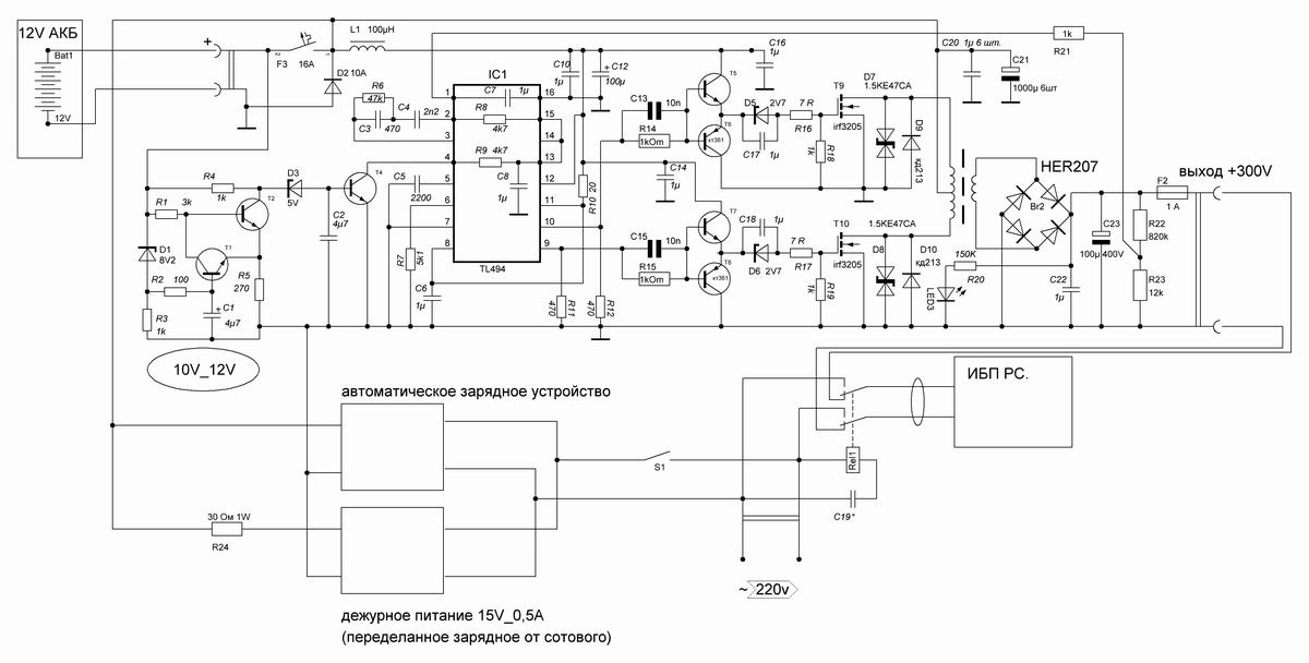
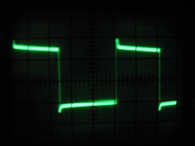
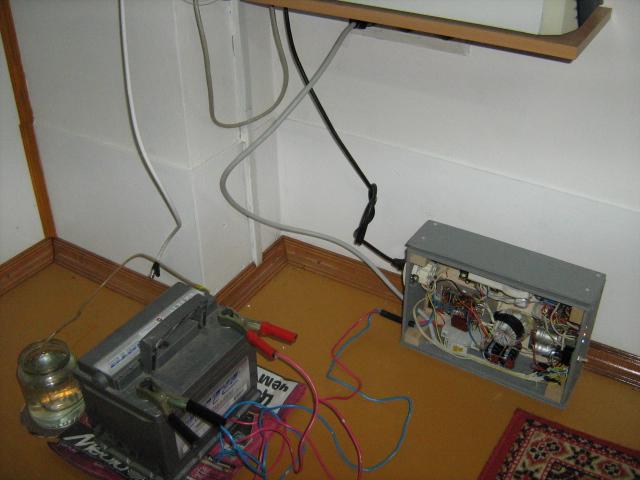
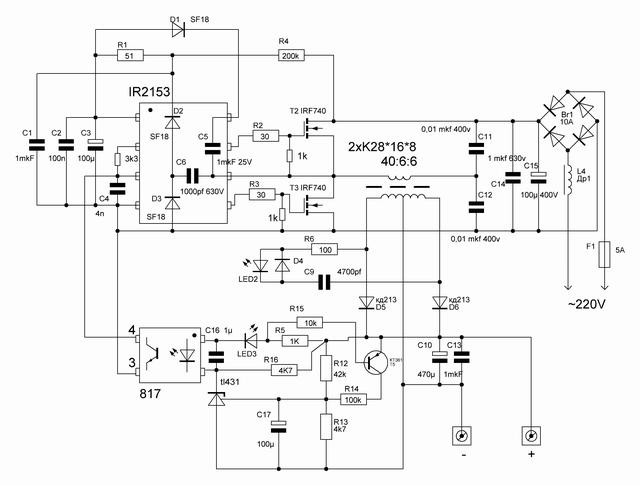
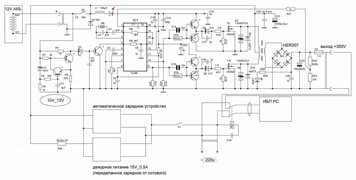
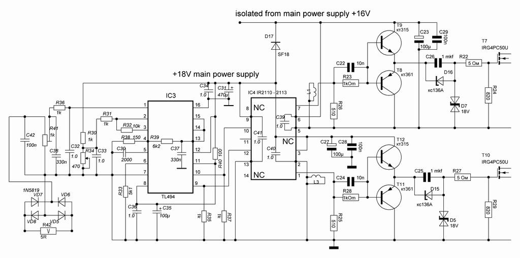
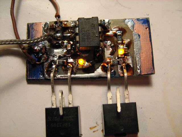
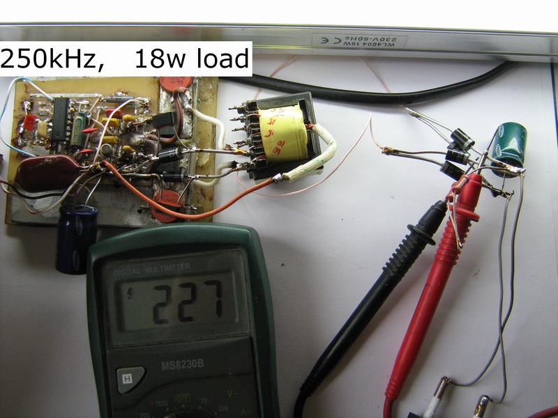
I've been working on a zvs driver circuit, whereby a tl494 drives a irf540 mosfet directly at 100kc's.
If I run the whole circuit on a single supply is runs fine, however if I use seperate power supplies for the tl494 and the mosfet load, and run the tl494 a few volts more than the load, the the mosfet runs considerably cooler, so much so to warrant further investigation.
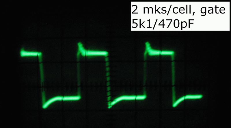
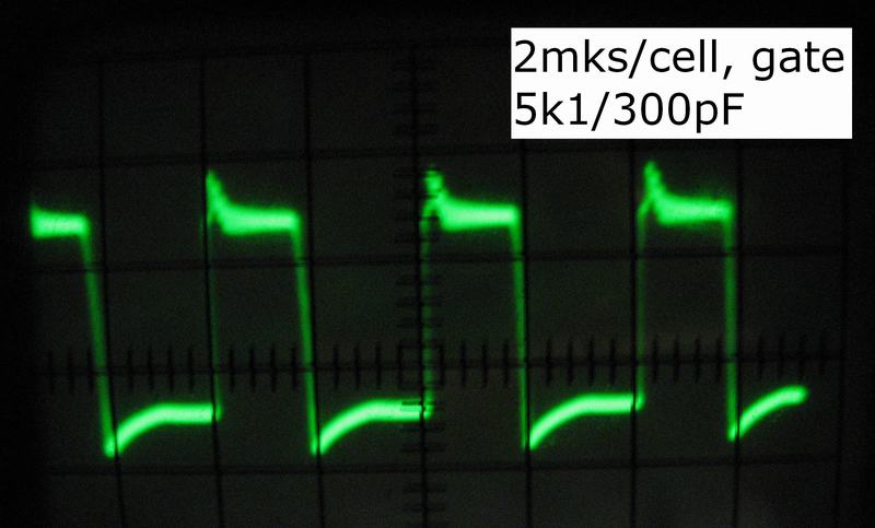
I'm making the assumption that the mosfet runs cooler with the gate drive being a higher voltage than the load due to the fact that the gate drive is able to achieve a faster switch on time by being able to overcome the gate charge quicker.
If I was to use a mosfet gate driver chip between the tl494 and the mosfet gates would I achieve a siilar improvemnt in efficiency?
 

Re: Mosfet gate drivers.

What supply voltage do you use (single supply)? May be you can post a link to the circuit diagram.
 

Re: Mosfet gate drivers.

12vdc 25amp, erm havent done a schematic, probably a good idea.
 

Re: Mosfet gate drivers.


so here is works quite well.
this is homemade ups for my sat-fish computer ).
 
Last edited:

Re: Mosfet gate drivers.

Hi,in your diagram you already have a buffer so you dont need any driver,the value of Rg determine your gate charge,you are using a centre taped transformer not H-BRIDGE,so you dont need a driver.
 

I got some 6 amp mosfet gate drivers to play with the circuit runs a lot cooler, without gate resistors theres is a lot of emi, 10 ohm resistors sort that out and the circuit still runs cool.
Seems that input capacitance isnt the figure to use, its gate charge when calculating switch on and switch off times.

Deep-n, you get up to a fair amount of building stuff, I like the ups, whats the giant mkt capacitor for in the centre?
 

whats the giant mkt capacitor for in the centre?
6,8mkF*250V, on lines of the feeding.
A surge value on key transistors powerfully depends from size and type of capacitor in feeding of the inverter and if capacity insufficient, supressors begin be powerfully warmed.

Apropos, fast automatic charger used in scheme (R14 75k, R13 necessary to select for task of the borders of switching 12,5 - 16V)
 
Last edited:

I see your circuit uses speed up caps on the bases of the fet drivers.

I found the issue I had in the end, I trusted the schematic I found on the net, mistake, the ciruit drove the fets directly from the output of the tl494, and without a resistor to ground, so obviously the fets would have charged up their gate capacitance and remained on during the off time, as the tl494 is a single ended transistor output in 'true' push pull mode, and they probably remained partially on so they would be in their linear region, no wonder the fets were effective heaters.
I found a couple of schematics that use a pair of complementary driver transistors emmitter coupled so I'll copy that.
I had tried to use mosfet driver ic's tc4224, but I just blew them up, I suspect latch up might be an issue when using these on breadboard, clamp diodes might have been a good idea I spose.
 

A case of difference between theory and practice:roll:. Here if you put a diode like IN4001, i'm sure it'll cure the problem as drawn in the diagram.
 

2 Dr pepper
circuit uses speed up caps on the bases of the fet driver
Previously than stop on this variant i tried different ways to driver connection.
Oscilloscope powerfully relieves adjusting the pulsed technology.
I think emmitter coupled complementary driver transistors much more reliable than driver ic's.

2 ALERTLINKS
i'm sure it'll cure the problem
sorry, this design works already month and problems meanwhile did not appear.
Possible appeared misinterpretation - I bore in mind "key transistors" equivalent FET.
 

I didnt get the diode idea, is the idea to isolate the supply spikes to the tl494's own circuit?

Deep'n I understand that circuit and I agree with your comment on fet drivers. What are the 2v7 zeners for to the gates of the mosfets, is the drive voltage too high for the fets or something.
 

2v7 zeners with c17(c18 ) and R18(R19) create negative potential on gates of switched off FETs, for increasing a noise-immunity.

Possible combine ic's driver and transistors. I have fired on various reasons several single IR2110, but nor one with emmitter coupled complementary driver transistors.
 
Last edited:

Thanks for the info.
I've never seen that done with zeners, a great idea, the zeners protect the gates from excess reverse bias, at the expense of losing 2.7v from the continuous positive drive, but with an 18v rail thats no problem.
I'll 'borrow' that idea on my circuit if thats ok, I tried a similar circuit, only the complementary transistor pair drive the fet directly through a 10r resistor, I have 2 1n4148's on the mosfet gate one to each rail to prevent excess voltage swing and latchup, it does however rely on the 100k pulldown on the mosfet gate for noise immunity, not terribly good.
I take it the 1uF before the gate is an mkt or polyester.
 

Its be well if this is useful.
Instead of zener diodes possible use led, so even looks better ).
25_1302266099.jpg
 

Yep, could change the voltage by selecting the colour too.

I see your not far from the black sea, I was out that way back in January, the parent compnay of the one here in the UK is in Finland.
 

I re-assembled my prototype using the caps and zeners on the mosfet gate, and it works well, there is noticeably less heat being dumped into the heatsink so it was worthwhile.
If I disconnect the feedback to the tl494 the circuit goes to max 50% duty cycle, however with no load the circuit pulls 500mA, if I replace the transformer with a carbon resistor, only energy being dumped into the resistor plus a tiny bit for the control circuit is used.
I suspect there is a little inefficiency involved when the transistors are switching an inductive load, some of that is going into the mov's accross the mosfets as they do get a little warm, the rest I suspect is due to the switching waveform slowing down when driving an inductive load, probably made worse by little more than pathetic construction compared to commercial designs.
 

In practice when battery is old, terminals are loose, excessive current drawn, strong ripple is developed on the dc bus.Many times it resets oscillator causing irregular outputs. Putting a diode in dc supply of ic and a big filter capacitor maintain steady dc supply and it helps solving the problem.
 

Hi DeepOne,

thanks for sharing your schematic and scope pics. Your schematic in the post #4 (TL494, push-pull) got my attention. Do i guess right, that the switching frequency is around 250kHz (2n2 and 5k1)? That would be quite impressive.
From the picture, your toroid transformer looks huge for that frequency. May i ask, why you choose such a big transformer? Because you had it already, or is there an other reason?

Thanks
 

Hi, Iwan_audio. Dimensionality of the picture from oscilloscope is 5V, 5 microseconds/ cell. So output frequency around 45kHz, frequency of the oscillator close to 100kHz.

why you choose such a big transformer? Because you had it already, or is there an other reason?
Ferrite ring is taken from CRT deflection systems of the small television set. Really, better core from that it is found under hand ).

Charger final version.


12_310 converter possible to try to do on IR2153 too ).


From curiosity tested scheme on frequency 160 and 250 kHz. Looks that works ok.
 
Last edited:

Thank you for the quick answer. I must be sleepy or drunk, when i look to the datasheet. Yeah, 45kHz makes much more sense.

I have analysed some Mosfet`s on Switching losses versus Rds losses for Push pull converter, see here
Mosfet_in_pushPull.jpg

From the point of efficiency, those fast mosfet like the PSMN017-60 would be perfect. It could even make 500kHz. But those sharp rising and falling times would also generate horrible EMI. For my planned 200W converter, i scare EMI and i plan to go with the IRFP3206, about 50kHz.

Could you tell me, what the schematic on the left side (T1, T2, T4) is doing? Its label'd as "10V_12V".

Thanks,
 

Status
Not open for further replies.

Part and Inventory Search

Welcome to EDABoard.com

Sponsor

Back
Top