DeepOne
Advanced Member level 2
- Joined
- Feb 26, 2011
- Messages
- 632
- Helped
- 99
- Reputation
- 200
- Reaction score
- 100
- Trophy points
- 28
- Location
- 45N39E, Russia
- Activity points
- 0
Follow along with the video below to see how to install our site as a web app on your home screen.
Note: This feature may not be available in some browsers.

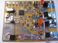
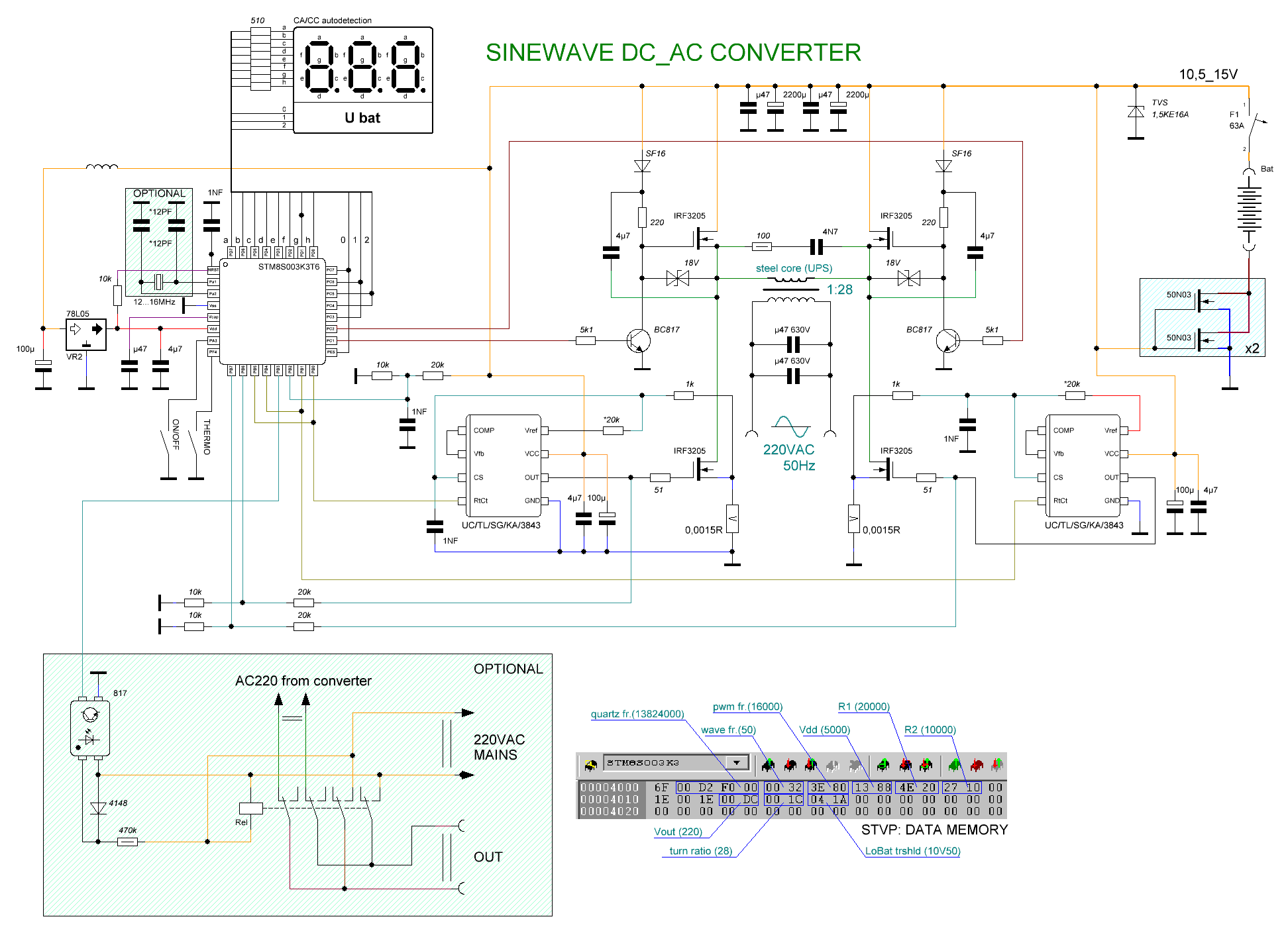
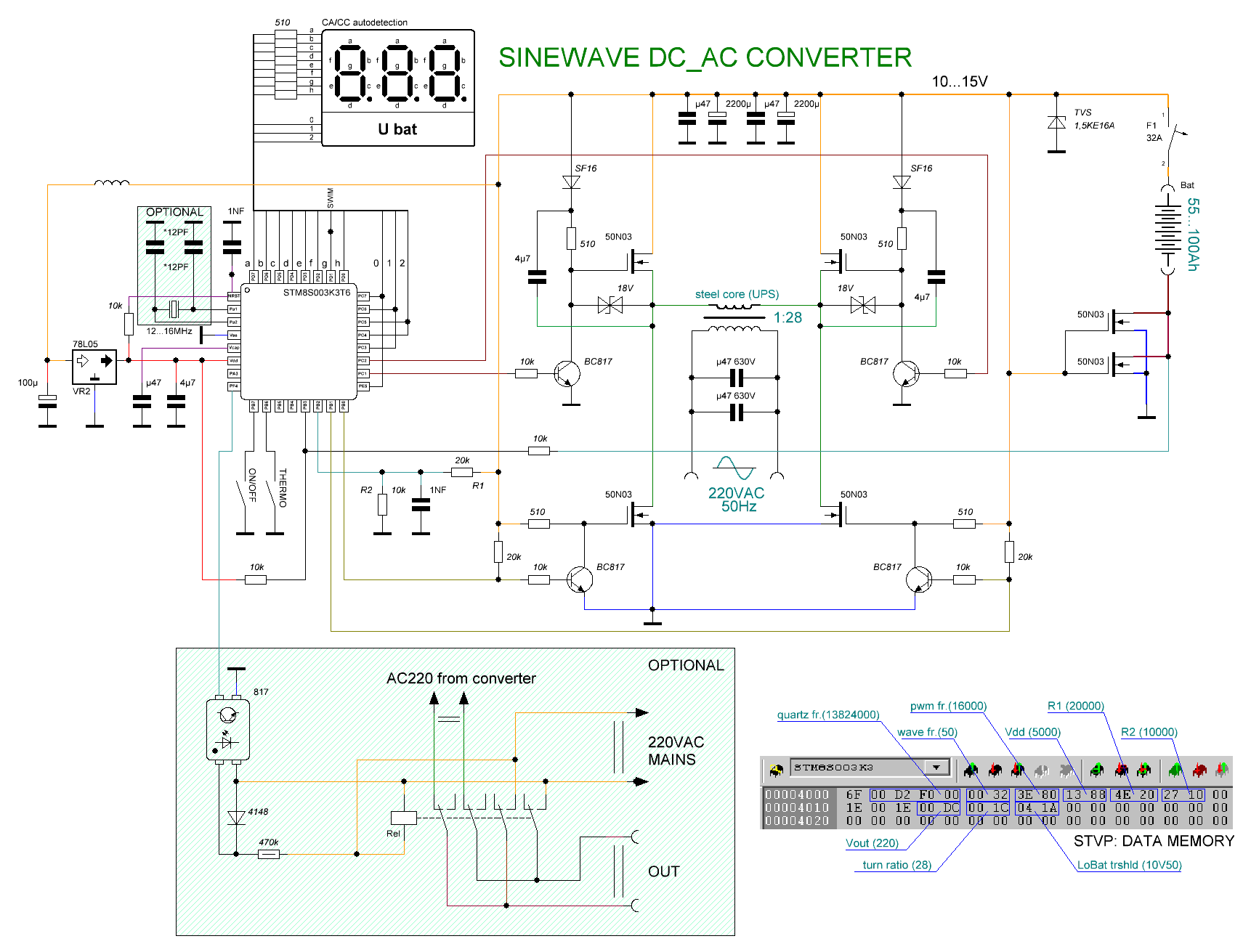
yes, but it is necessary to prescribe quartz frequency in eeprom as shown in circuit picture. or possible not to install quartz - in this case program is switch itself to use built-in RC oscillator.We can use many types of quartz (12-16MHz) without having to change the firmware?
better if mcu officially capable to work at used frequency. but in practice "8L" can work too at 16MHz under 5V.We can use different types of MCU Atmega8a-pu; Atmega8L-8PU; Atmega8L-pu
any type - mcu define this by itself.7 segment LED in the circuit using type common anode or common cathode?
that right but not essential.Differences in the 1k and 10k values in base BC817 in the two diagram. that's right or wrong?
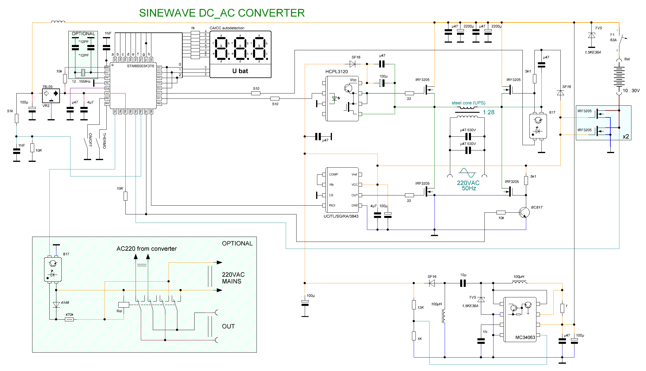


anyway it is necessary to check output frequency and signal on mosfet gates.I chose the correct frequency
when Vds near null V_AIN1 is near 1,6V so for activate protection Vds must be lower than -0,4V (1.6-1.2). that corresponds to 60...80А threshold current.smaller than 1.28vdc activate overcurrent protection.

so 5V on AIN1, right? try to adjust 2k2(from PB0 to AIN1) in range 2k2...510. but if overcurrent protection is operate may be there is some fault in circuit.then remove the 1k resistor
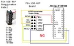
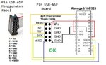
That is "SPlan 7".software that you use to draw the diagram
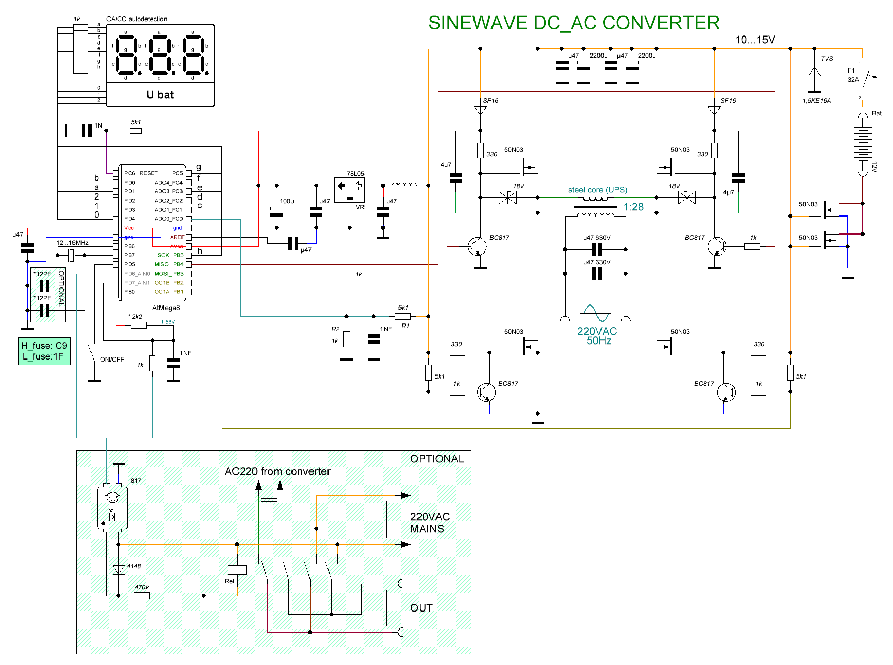
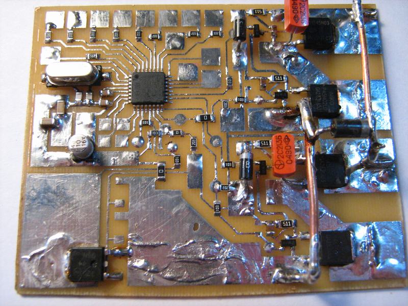
next prototype. 20W ACIM load test ok.