Continue to Site

Welcome to EDAboard.com

Welcome to our site! EDAboard.com is an international Electronics Discussion Forum focused on EDA software, circuits, schematics, books, theory, papers, asic, pld, 8051, DSP, Network, RF, Analog Design, PCB, Service Manuals... and a whole lot more! To participate you need to register. Registration is free. Click here to register now.

Sinewave inverter prototype...

Status
Not open for further replies.
that is experimental circuit, specifications exactly are not determined and depends from many things like transformer size or mosfet types.
 

After almost one day to find and fix errors. I finished, the circuit was run with the parameters: no-load current is 1A. Higher performance than using steel transformer. The mosfet very cool. I like it and will continue to test circuit DC-AC hight -voltage (310VDC-220VAC). I realized that when properly assembled according to the original scheme, not dropping components, I think anti-interference capacitors does not matter, but it is very important, common wire, too.
Thank Deepone many more.
Good wishes.
 

last version of this design with STM8 mcu, overheat and reliable overload protection. abandoned.
 

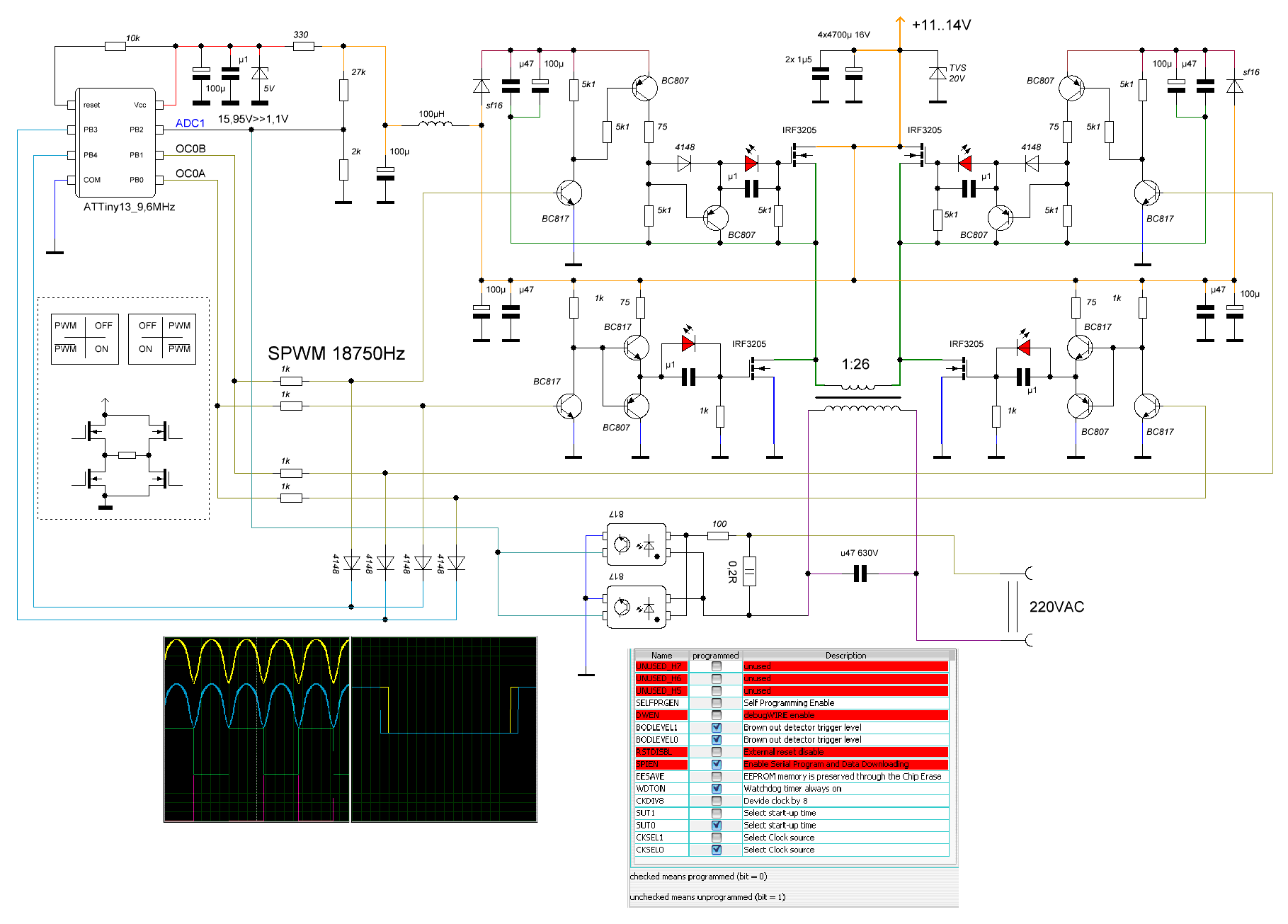
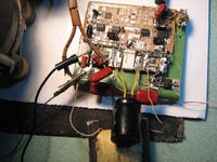
corrected version of tiny13 converter (only spwm for testing purpose, but it work).
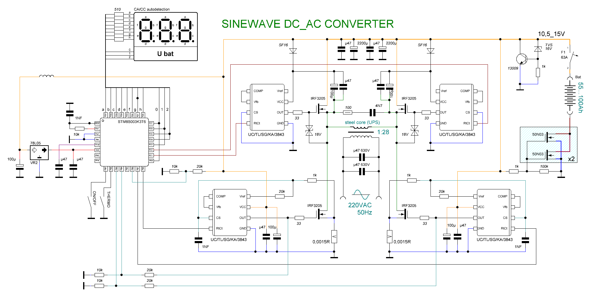
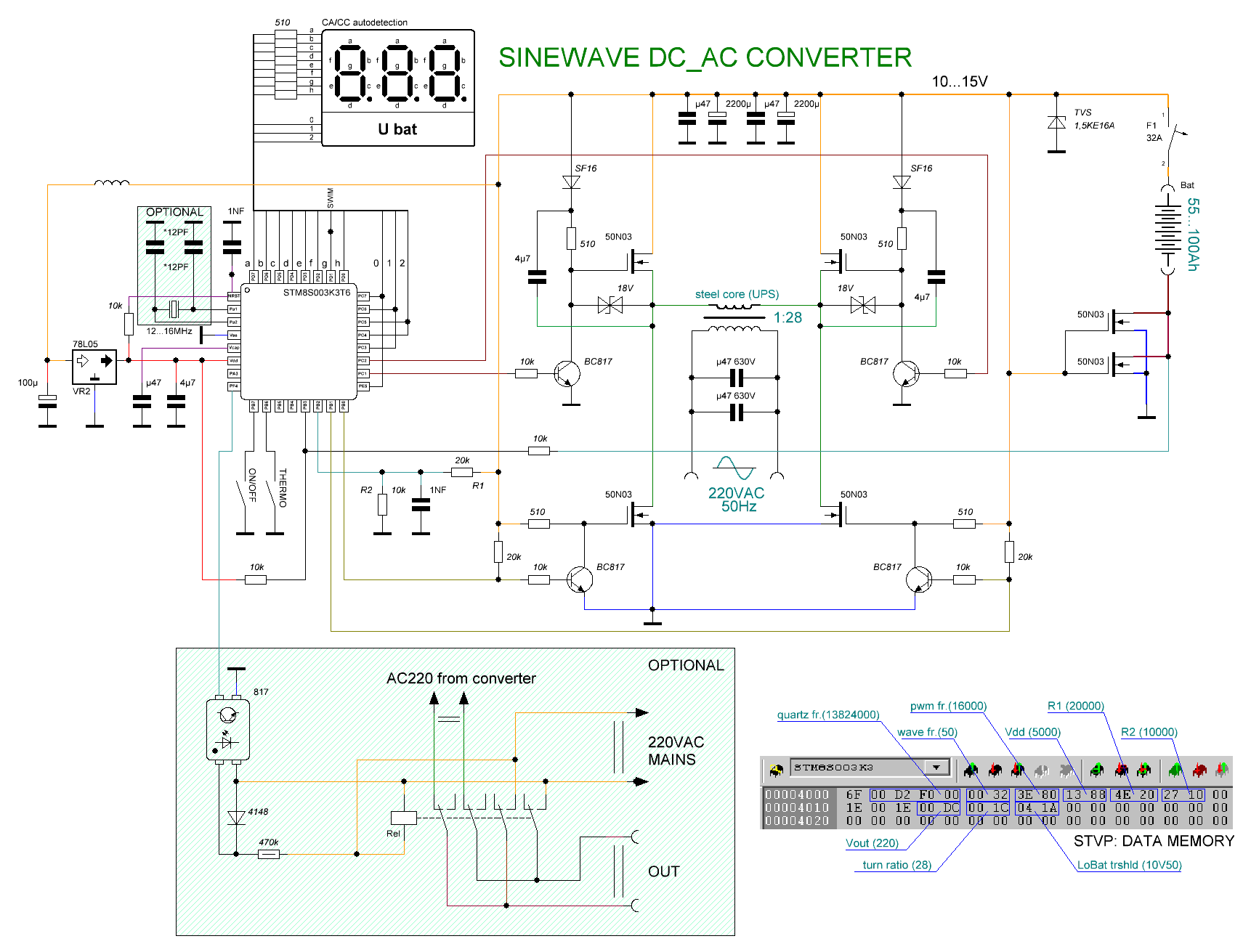
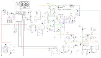
Dear DeepOne!
The type of transformer used is what type? ferrite core or steel core. Look at the frequency, I think that is a ferrite core. It is also possible to use both 2 kind?
Thank you!
 

Dear DeepOne!

Please help me find the reason why it does not work at the driver. I use the oscilloscope to check the pulse signal from MCU is well.

Thank you!
14370421_1795782327323710_4506303191473527621_n.jpg

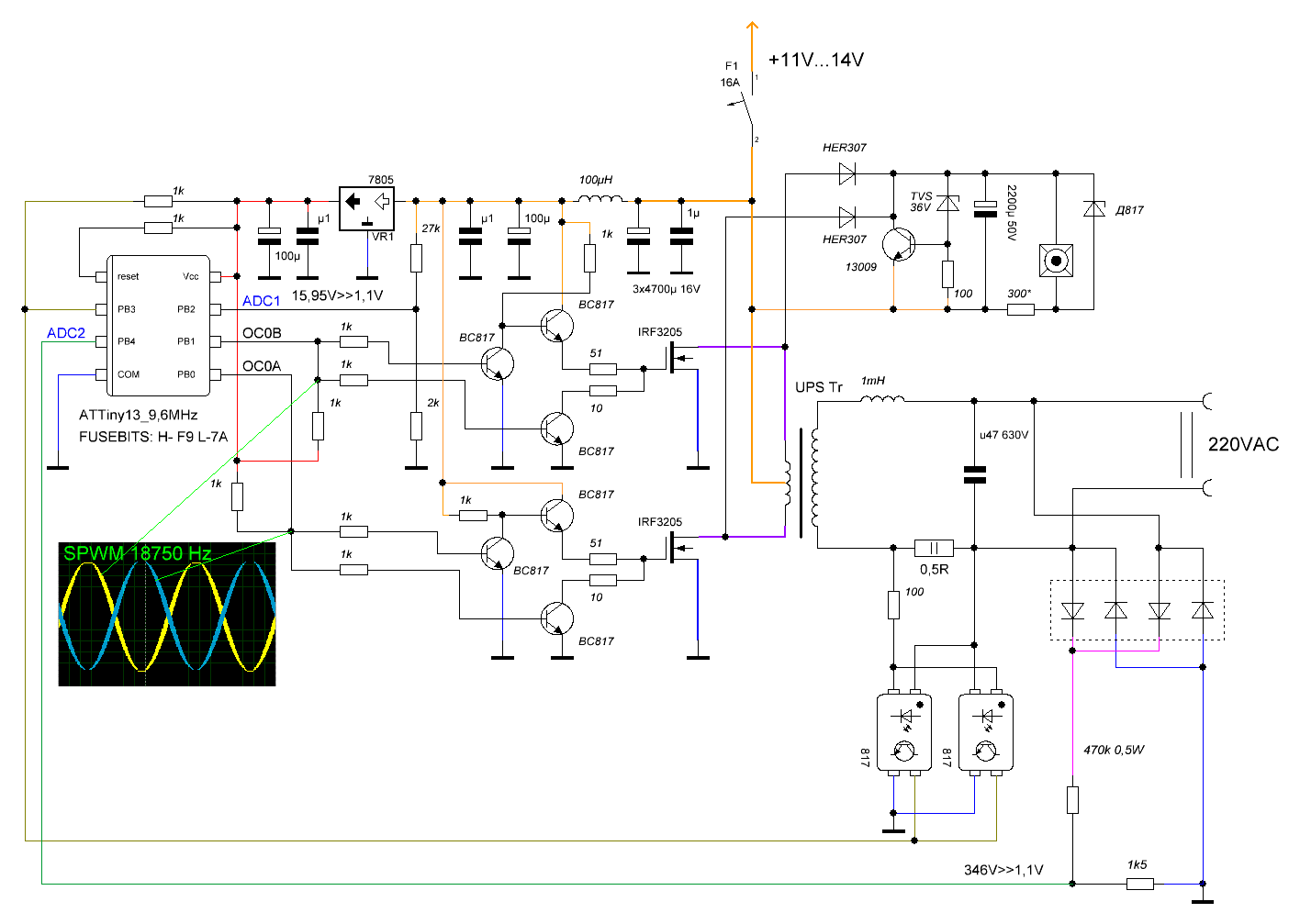
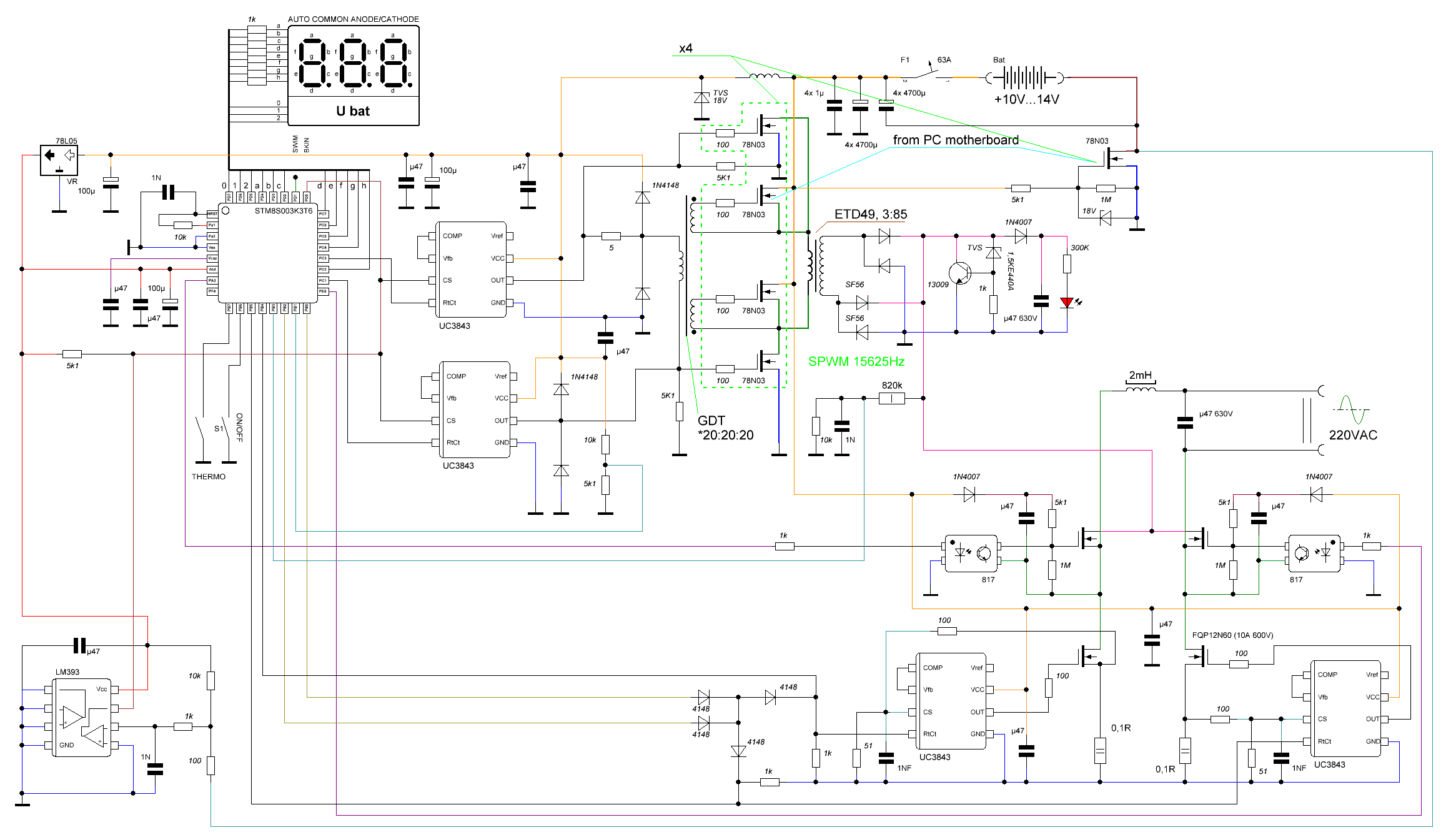
more complicated tiny13 circuit
 

this not very good scheme, good work is not expected from it anyway. but if you want you may trace this circuit point by point with oscilloscope.
 

Dear DeepOne

I tested with # 423 (IR2304 with totem pole) is pretty good match. Waveform, as shown below:
IMG_2946.JPG
But I tested with # 419 (IR2103 with no totem pole), the wave is distorted as shown below.
IMG_2945.JPG
See distortion, I mounted totem pole to the circuit IR2103, but destroyed mosfet. The circuit can not work.
Please help me fix # 419 using IR2103. Because in Viet Nam IR2304 it is very rare.

Thank you and happy weekend!
 

this distortion probably are result of the voltage correction subprogram work because tiny13 is not capable to recalculate smooth wave in real time.
i have no IR2103 and so have no possibility to check scheme in practice.
happy weekend for you too ).
 

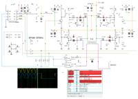
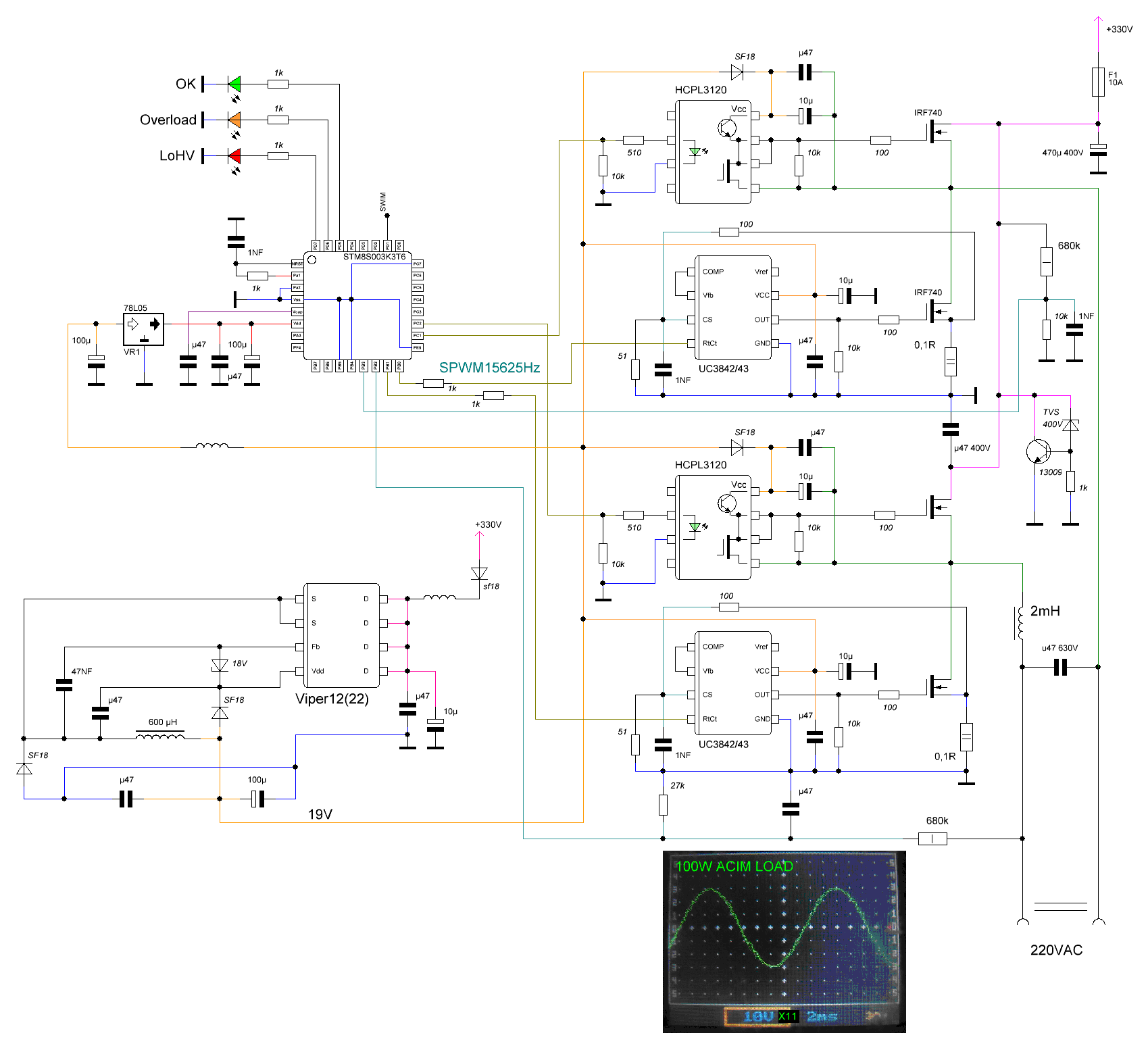
worked version of that HV modulator.

I have assembled as # 373, when loaded firmware software complete notification, but when I connect the 310VDC power supply, circuit does not work. Check with oscilloscope, there is no output pulse. Viper22 circuit is ok. 18.4VDC for drivers, and 4.8VDC for the MCU.
I'll have how to check ? There are other precautions during loading firmware? Please help me! Thank you!

IMG_2951.jpgIMG_2950.jpg
 

in this circuit mcu is not generate pulses in three cases - when start, voltage on adc3 (PB3) is lower than (Vdd/255)*207 (3,9V if Vdd=4,8); in work mode when adc3 input < (Vdd/255)*184 (3,5V) or when PB2 < Vdd/3.
 
Last edited:

The key to understand failures is to understand the non-ideal characteristics of your layout and each component against assumed V:I(t) response. This includes primary core saturation, wire inductance, inductive and capacitive stray coupling, effect of Common Mode noise on differential induced noise, and the benefits of CM chokes. (ferrite beads around conduction pairs)

All high current paths must become balanced by twisting the DC in with return together. Examine the current loop of your layout and minimize the area of the loop ASAP.

In order to monitor power consumption you need a reliable DC current shunt < the RdsOn of your drivers (6 mOhm) I would suggest 1 mOhm ground side, low-ESL, current shunt using magnet wire. To make a non-inductive wire shunt, I use magnet wire , folded twisted so the ends are together then the inductance cancels out. Then add a connector to the board to your common ground point ( BNC bulkhead receptacle) so you can attach 50 Ohm coax from board to scope and terminate the coax with 50 Ohms at the scope using a BNC T connector ( if not avail. in scope) This will give the cleanest DC current sensing possible to monitor overcurrent conditions. ( YOu can build an OCP circuit to automatically shutdown and protect your expensive parts. ( Over current protection)

Since AWG 20 is 33 mOhm/m to make 1 mOhm you need 30 mm of AWG20 magnet wire or thin insulated wire, folded in half, twisted 5 times or more and connected close to your star ground system to your supply return. If you can use a lab supply to put in a calibrated 10A CC limit or any low voltage , you can verify/calibrate the mOhm shunt with a DC meter.

From this point on it is important to view every high speed LdI/dt wire as a potential voltage drop and examine why the more expensive drivers that are 10x faster response work better in order to make the slower cheaper ones work safely without cross-conduction MOSFET failures.

Understand what makes them slower and how that affects MOSFET power dissipation.
How can you speed the gate drive transition to protect the MOSFETs by switching Vgs faster?
How does the dead-time change and how do you control it?
 

in this circuit mcu is not generate pulses in three cases - when start, voltage on adc3 (PB3) is lower than (Vdd/255)*207 (3,9V if Vdd=4,8); in work mode when adc3 input < (Vdd/255)*184 (3,5V) or when PB2 < Vdd/3.

According to your guidance, I checked PB 3 = 4.5v, but it did not work. Then I connect PB3 and PB2 to Vdd = 4.8V, but it also does not change.
I have reloaded firmware mode "Read out protection OFF" under the Option byte. Bulbs do load was light, but less than 1 sec two mosfet source controlled by PB1 and PC2 was short. The two remaining are still good.
I think the first time I had to load firmware mode Read out protection ON , so the circuit is not working.
After reloading firmware. The circuit was running but I have yet to find any place that may damage the mosfet. Was two times instead mosfet but I do not have enough time to measure and inspect circuit parameters.
Pleased to receive additional instructions. Thank you!
 

in my test overcurrent protection of this circuit is reliable even if mcu generate wrong signal to mosfet drivers. i think your pcb layout does not be fit for high voltage application. anyway, better do first test with low voltage on bridge, such as 24 or 36VDC.
_____________
test microprogram for this circuit. simple generate spwm, without voltage measurement.
 

Attachments

  • test for stm8s003.zip
    5.5 KB · Views: 134
Last edited:

next prototype. 20W ACIM load test ok.
 

Attachments

  • c_hex_pcb.zip
    102.6 KB · Views: 144

Status
Not open for further replies.

Part and Inventory Search

Welcome to EDABoard.com

Sponsor

Back
Top