Continue to Site

Welcome to EDAboard.com

Welcome to our site! EDAboard.com is an international Electronics Discussion Forum focused on EDA software, circuits, schematics, books, theory, papers, asic, pld, 8051, DSP, Network, RF, Analog Design, PCB, Service Manuals... and a whole lot more! To participate you need to register. Registration is free. Click here to register now.

Simetrix 3phase inverter

Status
Not open for further replies.

enki22

Newbie
Joined
Oct 29, 2022
Messages
5
Helped
0
Reputation
0
Reaction score
0
Trophy points
1
Activity points
35
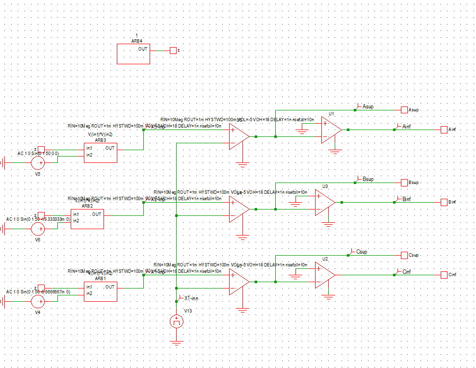
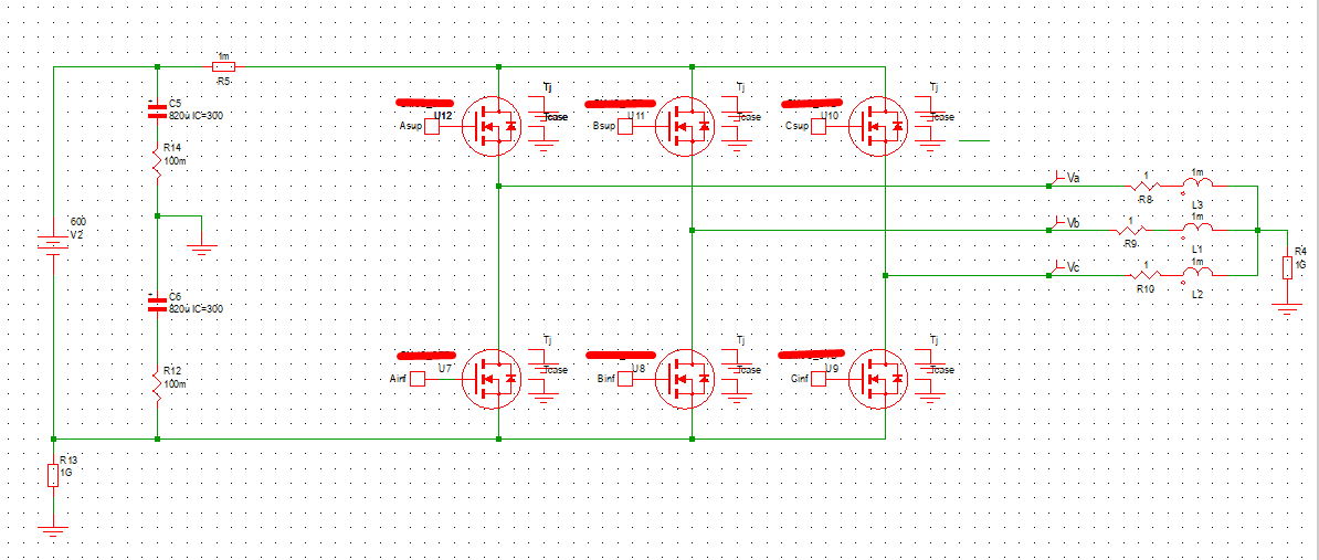
Hi guys, i am trying to make a three phase inverter on simetrix, but the output voltages and currents are totally wrong and very often it gives convergence error if i try to modify something. I don't understand what I'm doing wrong, maybe a more experienced eye could help me.

p.s: the sinusoidal pwm circuit seems to work fine so i suppose the problem is in the inverter circuit
bb.png
aa.png
 

Hi,

There are dedicated MOSFET drivers. For a good reason.

If this schematic is your idea: Please read application notes on how to control HIGH side and LOW side MOSFETS for power applications properly. Every MOSFET manufacturer as well as every MOSFET_driver manufacturer provides them for free.

If this schematic is from an internet source: please provide a link to the site.

Klaus
The schematic is my idea, the mosfet are dedicated, the sinusoidal pwm is done to match the requirements of the datasheet
I even tried with other switches and i have the same results in output, so i was wondering if the problem was on the circuit of the inverter itself
you think i should chek better the sinusoidal pwm ?
 

Hi,

again:
Learn how to control MOSFETs, especially HIGH side.
--> Use dedicated MOSFET drivers.

More detailed:
A MOSFET is ontrolled by V_GS = the voltage between Gate and Source. Source, not GND!
I don´t see your high side drivers to use the SOURCE voltage at all. Dedicated High side driver use the SOURCE voltage.

Klaus.
 

I see the post #1 simulation circuit as a behavioral design, not the simulation of a real inverter. As KlausST stated, the gate voltage has to be applied between gate and source, this can be either achieved by a real gate driver model or simply a controlled SPICE voltage source. Another problem is missing dead time between high- and low-side switches.
 

I see the post #1 simulation circuit as a behavioral design, not the simulation of a real inverter. As KlausST stated, the gate voltage has to be applied between gate and source, this can be either achieved by a real gate driver model or simply a controlled SPICE voltage source. Another problem is missing dead time between high- and low-side switches.
Unfortunally they dind't give me the datasheet, they give me only the txt file and some specification, it's my first time with simetric i only used psim and simulink, so i am a lot confused, I've only dealt with behavioral design so i don't know where i could learn how a real schematics is.

I've found this on the internet and if i put my mosfet there, the circuit works O_O
 

Hi,

again:
Learn how to control MOSFETs, especially HIGH side.
--> Use dedicated MOSFET drivers.

More detailed:
A MOSFET is ontrolled by V_GS = the voltage between Gate and Source. Source, not GND!
I don´t see your high side drivers to use the SOURCE voltage at all. Dedicated High side driver use the SOURCE voltage.

Klaus.
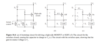
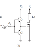
I used a npn pnp gate drivers for the low side, and a bootstrap for the high side switches, should be right or it's not correct ?

risultato buono.png
 

Hi,

I've never seen a high side drive like this. I did'nt go into detail, but it still refers to GND, which I told you already is the wrong way.
So you did not follow my recommendation. You did not communicate why. You did not communicate which application note the idea/circuit is from.
I guess you will have your reason for this.

Simple question:
Does it work as expected?
* yes: be happy
* no: re read my posts. Follow what I have told you

Generally:
It's your job to look fir datasheets. When I get an electronics design job, it's quite common that nobody gives me a datasheet and nobody does the internet search for me.

You have the simulation tool. You have the schematic. And you have the expectation/idea how your circuit should work.
So it's the easiest way that you use the simulation to find out whether it does work as expected or not.
If it does not work as expected: give complete informations, like
* what did you expect?
* how did you test it?
* what is not like expected?

Give links to datasheets and application notes you used to design this circuit.

I'm interested in finding a solution fast. I'm not interested in repeating informations an lengthy threads.
I recommended to work through application notes. Maybe these application notes are 10 pages or more, thus it should be clear that the information can not be compressed in a couple of lines in a post reply. You have to do some work on your own - like every electronics designer.
I read many datasheets per day and have a lot of my knowledge from thousands of application note pages
A forum can't replace: school, doing internet search, reading documents.

Klaus
The problem is this, i don't have a datasheet, beacuse the nmos used is a general model that my professor gave to me, it's not a real nmos i can find in some company site. As an high side gate driver I used what i find in the book Power electronics by daniel w. Hart, same applies to the low side. On the internet i've found nothing on the gate driving topic (i find only behavioral schemes or schematics with integrated circuit). I don't have any specification to respect, the project need only to trasfrom dc to 3 phase ac (wich looks like it's doing) but I am not sure is the correct way of doing it, or if the three phase current waveform i get in output are what i should get or are some random results.
The circuit is done by me i have no application notes the only things I used are this gate drivers circuit taken from the book (that i searched following your advice), it's a normal schematics of an inverter, while the circuit on top is a SPWM that i made with the confrontation of a triangular waveform and a sinusoidal waveform (like every basic SPWM).
 

Attachments

  • a.png
    a.png
    78 KB · Views: 122
  • b.png
    b.png
    10.4 KB · Views: 112

Hi,

The problem is this, i don't have a datasheet
My point of view:
You don´t read the posts and you don´t communicate.

The MOSFET datasheet isn´t the problem at all. And I did never ask about the MOSFET datasheet.

***
I recommendend you to use a dedicated MOSFET driver. And apparently you never did an internet search or a forum search about "mosfet driver".

On the internet i've found nothing on the gate driving topic (i find only behavioral schemes or schematics with integrated circuit).
This is nonsense. It´s one of the most often discussed electronic topics. Here in this forum as well as in the internet.
My internet search for "high side gate driver circuit" gives almost 30 million hits.
30 million is not "nothing"!

There are many thousands of examples, tutorials, documents, even videos on how to design a "complete" sinwave PWM inverter. Many more of you just look for details, like "half bridge"

The shown circuits most probably are for low voltage DC (maybe up to 20V) and low frequency switching. None of them shows your situation with combined HIGH side + LOW side which is called half bridge. None of them is for high frequency PWM (in the kiloHertz range).

****

I guess it´s time for me to leave it to others to assist you. (I´m not angry, I just don´t want to spend that much time on one thread)

Good luck.

Klaus
 

* You need to confirm current flows through mosfets at the proper times. Also through each load at the proper times.

* Make sure a half-bridge never has current shooting through both mosfets simultaneously.

* Make sure a mosfet receives proper bias so that it turns on entirely, and shuts off entirely.

Your load resistors appear to be 1 ohm. Change this value so it draws, say 1 or 2 Amperes.
 

Status
Not open for further replies.

Part and Inventory Search

Welcome to EDABoard.com

Sponsor

Back
Top