Continue to Site

Welcome to EDAboard.com

Welcome to our site! EDAboard.com is an international Electronics Discussion Forum focused on EDA software, circuits, schematics, books, theory, papers, asic, pld, 8051, DSP, Network, RF, Analog Design, PCB, Service Manuals... and a whole lot more! To participate you need to register. Registration is free. Click here to register now.

Sample and Hold Circuit, cant get the same waveform!

Status
Not open for further replies.

syee10

Member level 3
Joined
Apr 2, 2010
Messages
63
Helped
1
Reputation
2
Reaction score
0
Trophy points
1,286
Location
Malaysia
Activity points
1,758
Hi all,

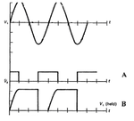
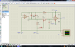
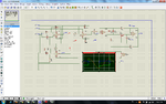
I am designing a simple sample and hold circuit where the input is a sinusoidal analog input and it is control by a TTL compatible square wave (waveform A). The result waveform i should get is waveform B in the attach file but i tried a millions time i still cant get the same waveform. Someone there can help me out? I had attached all the file in the attachment..
 

Attachments

  • SH1.png
    SH1.png
    20.1 KB · Views: 112
  • SH2.png
    SH2.png
    126.5 KB · Views: 136

Re: Sample and Hold Circuit Help!!

You mean a problem in simulation or in the real circuit? What's the observed waveform? What's the voltage at the (COM) node?
 

Re: Sample and Hold Circuit Help!!

Can you post the DSN files?
 

Re: Sample and Hold Circuit Help!!

I mean simulation not practically testing the circuits...
 

Attachments

  • Part7.rar
    32.4 KB · Views: 80

Re: Sample and Hold Circuit Help!!

When the switch is OFF the gate of the FET is floating. The gate needs to go somewhere.

Keith.
 

Re: Sample and Hold Circuit Help!!

When the switch is OFF the gate of the FET is floating.
Yes. Gate bias of a JFET is a bit more complicated than of a MOSFET. You would connect a voltage divider (equal resistors) from U1A and U1B output to the gate to set the FET on state voltage and apply negative supply voltage V- to the gate to switch it off.
 
Re: Sample and Hold Circuit Help!!

I dun really understand wat you mean..perhaps u can draw me a connection XD
 

Re: Sample and Hold Circuit Help!!

I guess FvM means like this. It doesn't actually work like the diagram you showed, but that is because your circuit doesn't work on the negative half of the sine wave - this one does.

Keith.
 

Attachments

  • Sample & Hold 2.pdf
    14.7 KB · Views: 111

Re: Sample and Hold Circuit Help!!

Yes exactly, thank you. The switch S1 can be also replaced by a diode (anode at the gate), setting the control voltage to a negative polarity.
 
Last edited:

Re: Sample and Hold Circuit Help!!

Can i know what kind of switch (S1) you are using? Why is there a ground at the switch?
 

Re: Sample and Hold Circuit Help!!

I have had the "pleasure" of designing a JFET based S/H
product once.

The key is to ensure that when "on" the JFET switch gate
is roughly at the sampled signal potential, and when "off"
it is pinched off as little as possible, beyond "what works"
so you minimize charge injection and sampling pedestal.

I did this with a secondary follower amp (following both
sides of the switch, because pinchoff needs to comprehend
both and you don't know beforehand or during subsequent
input deviation during hold, which). The gate switched
between min(VIN,VHOLD) and min(VIN,VHOLD)-VPset (a
PJFET process).

You could of course pinch it more severely but that makes
the Qgate and sampling pedestal common-mode-sensitive.
 

Re: Sample and Hold Circuit Help!!

Can i know what kind of switch (S1) you are using? Why is there a ground at the switch?

It is a voltage controlled switch. It has two input terminals and two output terminals. I guess it is a bit like a relay in that respect. The ground node is there because otherwise the switch would be floating.

Keith.
 

Re: Sample and Hold Circuit Help!!

The voltage controlled switch is a simulation tool rather than representing a real component. You can set threshold voltage, Ron and Roff according to your requirements. Unlike a real switch, it has no voltage limitation or charge injection, you can use it for pA or kA as well.
 

Re: Sample and Hold Circuit Help!!

keith,

Can you check whether is my connection correct in SH3? I need to get an output just like the waveform 'B' in SH1.The output of inverter U5 is my reference TTL square signal. The waveform in SH1 is only show the positive part of Y axis. What i should get is the signal being sampled when the signal 'A' in SH1 is positive and hold the signal when the signal 'A' in SH1 is negative. Then the output will be the waveform 'B' in SH1. The connection that i constructed in SH3 seems to be the opposite of what i want..

I also attached the DSN file of proteus..hope to get your reply soon. Thanks =)
 

Attachments

  • SH3.png
    SH3.png
    143.2 KB · Views: 105
  • SH1.png
    SH1.png
    20.1 KB · Views: 99
  • Part8.rar
    27.4 KB · Views: 71

Re: Sample and Hold Circuit Help!!

Simply remove the inverter U5, or add another one. That will reverse the sampling logic.

Keith.
 

Re: Sample and Hold Circuit Help!!

Can the sample and hold circuit change some configuration? because i must place an inverter U5 at there to get the correct waveform..
 

Re: Sample and Hold Circuit Help!!

Maybe the output of U2 isn't sufficient to drive your switch? Monitor the output of U2 and see. You can always edit the switch parameters. Bear in mind the switch is a "perfect" one. If you want to build this circuit you will need to find some circuitry to replace it.

Keith.
 

Status
Not open for further replies.

Part and Inventory Search

Welcome to EDABoard.com

Sponsor

Back
Top