Continue to Site

Welcome to EDAboard.com

Welcome to our site! EDAboard.com is an international Electronics Discussion Forum focused on EDA software, circuits, schematics, books, theory, papers, asic, pld, 8051, DSP, Network, RF, Analog Design, PCB, Service Manuals... and a whole lot more! To participate you need to register. Registration is free. Click here to register now.

Ripple in rail voltage of H-Bridge

Status
Not open for further replies.
Thanks everyone for the reply.

It is unlikely that the readings are due to EMI at 200KHz. Readings due to EMI pick-up generally diminish by reducing the loop area of the oscilloscope probe terminals. I had varied the loop area of the probe a great deal but the readings didn't show even the slightest of change.

I suspected the ripple to be a glitches at 200KHz, but the waveform is too even and smooth and is more likely ripple than glitch.

The ripple is probably due to the ESL of the electrolytic capacitors.
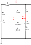
The inductance due to the loop formed by 2cm long leads, placed 1.5cm apart is roughly 45nH.
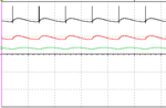
Here is the simulation result after putting a 45nH in series with the electrolytic capacitors and 1nH in series with ceramic capacitors.

RED: Ceramic cap voltage (V2)
GREEN: Electrolytic cap voltage (V1)
BLACK: Rail voltage (V3)

- - - Updated - - -

The electrolytic caps are hardly absorbing any current, their voltage is almost constant and not much effected by the ripple in the rail.
 

Attachments

  • Capture2.PNG
    Capture2.PNG
    6.8 KB · Views: 64
  • Capture3.PNG
    Capture3.PNG
    3.6 KB · Views: 57

You are showing simulation waveforms, so you get out what you put it.

The waveform show what can be expected for a specific bus load current. The only remaining question from my side: What's the purpose of this thread?
 

Take a look at the black and red waveforms. I understand this is only simulation. Ignore the spikes on the black trace for the time being. V2 and V3 are essentially same except for a level shift. The black spikes are effectively filtered by L3. V1 is effectively filtered by large C2. What is the waveform at R1-L1 junction? All these are expected - imho.
 

Really you need quality film/foil caps near the H bridge, electro's with long leads do not cut it at 100kHz or higher, generally they are resonant at these frequencies, OK if paralleled with quality film caps, or you choose just the right ones (lowest can height) and parallel quite a few with short leads right at the H bridge, its called power electronics layout and is generally only learned by trial and error...
 
The waveform show what can be expected for a specific bus load current. The only remaining question from my side: What's the purpose of this thread?

This is a very good thread. It is a good example of how important PCB layout and component selection is. His measured and observed data is proving theory.
 

The input capacitors must absorb all the current in the leakage inductor of the transformer, each time the transformer reverses its polarity. If the capacitors have low ESR, there is hardly any power wasted during each ripple cycle. So a another question would be:

What at all is the need to reduce the ripple? (As long as it is safely below the breakdown of the MOSFETs)

Reducing ripple is only wasting space that is occupied by aluminium caps. Why not just place only ceramic caps enough to limit ripple to say 2V pk-pk.
Calculated value of capacitance to limit ripple to 2 volts is around 100uF only.
 

The input capacitors must absorb all the current in the leakage inductor of the transformer
The "current in the leakage inductance" is the actual output current, which is present with or without leakage. Leakage inductance is helping to smooth the output current peaks caused by rectifier reverse recovery.

What at all is the need to reduce the ripple?
Good question. There's no absolute need, but I see some reasons though
- reducing EMI. A commercial device complying with respective regulations needs to.
- increasing efficiency by avoiding additional battery and cable losses according to the ripple caused RMS current
- keeping the current rating of the filter capacitors
 
I must admit mrinalmani, you could solve a lot of your questions by making a representative simulation in LTspice, put your transformer in there with the same leakage, its not perfect, but its very good as long as you realise limitations.
I also attach a pcb layout guide, and a simple basic full bridge sim to get you started.
 

Attachments

  • Basics of SMPS Layout _4.doc
    645.5 KB · Views: 70
  • Full Bridge.txt
    9.3 KB · Views: 39
Thank you Treez!

FVM: Thanks you for suggestions.
However, the three points you mentioned about keeping ripple low are slightly doubtful.

1. Reducing EMI:
A perfect square wave with sharp edges will have much more higher order harmonics than curved square wave resulting due to ripple. (Insinuating Better EMI performance?)

2. Reduction in ripple current.
It appears to me that the ripple current in full-bridge transformer application is independent of the input capacitance, dictated only by the leakage+stray inductance.
Each time the transformer voltage reverses, the current in the leakage inductor must reverse its direction. The capacitor must sink this current till it decays to zero and then source it back till it rises to the same value (but opposite direction in the inductor)

Thus the amount of ripple current seems to depend only on the magnitude of load current, leakage value and switching frequency. Higher value capacitor will lead to lower ripple voltage but not current.

- - - Updated - - -

The whole propose of this thread was to discuss how the rail voltage in a generic full-bridge application is made almost free of ripple. And now another question has come up: "Why at all does the rail voltage need to be low on ripple?"
 

Why does it need to have low ripple, good point, if it does the job, ie drives the load satisfactory, and the peak of the ripple doesn't damage anything, then who cars about the ripple.
I remember once we had a input current regulated sepic which could drive the 5W led load fine even if it had just 100nf of output capacitance....but if you had no output capacitance, then the output voltage would spike real high and damage stuff.

Square waves do have higher freq harmonics, but that means you have digher di/dt's to worry about, so its worse.
I think you need to jump on the free ltspice simulator to answer many of your problems.
 

There will be no ripple on the input rails only if the source impedance is ZERO. We shall try to reduce the ripple so that it does not interfere with other devices. Ripple will always tend to get averaged out when it reaches another device. Most devices are ripple tolerant to some extent.

High spikes are a different beast altogether. They love to get coupled wirelessly and we should try to remove the sharp spikes as much as possible. They have also very rich harmonic content and can interfere with many communication systems. Again, a square wave exists only in idea.

A battery is almost an ideal capacitor: it has a 'bad' dielectric: why do we need so many capacitors in parallel with the source? Reducing source impedance to VERY small value is also not really desirable because switching will produce strong spikes. What I mean is that di/dt must be under control (not by gate capacitance but by source impedance).

ESR of capacitors should be small, but not zero! That will mean that charging and discharging should be under control of the designer.

A small inductor in series with the source current also provides a soft start!

We need to use the imperfections to our advantage.
 

Most often the "high spikes" you see are CM (common mode) pick up of your scope, they are not really on the bus.

To test this compute the current needed to give a 5V spike in 20nS on a 100uF cap, i/C = dV/dt

i = 25kA, 200nS = 2.5kA, 2uS = 250A

All pretty plainly ridiculous except for very high current circuits, of course wiring inductance and ESL of caps can contribute to V spikes on fets right at the fet,

one way to test is to short your scope probe and attach it to various points and see if the spikes are still on the screen, if they are then you can subtract them from "real" measurements to give you a better idea of what the overshoots really are.

I look forward to your reporting back...
 
I just thought of something else. A 12 volt battery implies automotive use. If we start calling ripple current noise and understand it is on the power lines from the battery then there may be a automotive spec for the amplitude of the ripple.
 

Status
Not open for further replies.

Similar threads

Part and Inventory Search

Welcome to EDABoard.com

Sponsor

Back
Top