Welcome to our site! EDAboard.com is an international Electronics Discussion Forum focused on EDA software, circuits, schematics, books, theory, papers, asic, pld, 8051, DSP, Network, RF, Analog Design, PCB, Service Manuals... and a whole lot more! To participate you need to register. Registration is free. Click here to register now.
Please find the attached document for the BiCMOS Inverter and clear my doubts. I have posted the entire explaination of the same and at the end there are 2 questions.
In the text it says that in condition 1 , Capacitor charges to Vdd-Vbe , i.e assume 5-0.7 =4.3 and then it fully charges when Q2 cuts off, As per your reply , Vdd-Vc<Vbe2 and Q2 is off , How?, What is the value of Vc here?
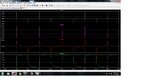
Please find enclosed here with the simulation waveform of the circuit:
The enclosed waveforms starting from bottom indicate 1) MoS Inverter output 2)The current waveform thru Resistor(5K used) placed across top BJT Emitter base (This shape also indicates the Emitter base Voltage wave shape).3)Base current of top BJT 4) Current thru the Load capacitor.
From the waveforms we observe that the PMOS Drain drives current thru { Resistor(5K used) and top BJT Emitter base combination } into the load capacitor.The BJT will conducts when its Vbe is greater than cutin voltage and charges capacitor thru collector emitter within a short period.
once the capacitor is fully charged, as there is no more charging current thru resistor, there by no Vbe(cutin) potential and hence BJT will be in cut off for rest of the cycle period.
This site uses cookies to help personalise content, tailor your experience and to keep you logged in if you register.
By continuing to use this site, you are consenting to our use of cookies.