Continue to Site

Welcome to EDAboard.com

Welcome to our site! EDAboard.com is an international Electronics Discussion Forum focused on EDA software, circuits, schematics, books, theory, papers, asic, pld, 8051, DSP, Network, RF, Analog Design, PCB, Service Manuals... and a whole lot more! To participate you need to register. Registration is free. Click here to register now.

[SOLVED] Question about a multiplexer based bus.

Status
Not open for further replies.

ammar_kurd

Junior Member level 3
Joined
Aug 7, 2015
Messages
31
Helped
0
Reputation
0
Reaction score
0
Trophy points
6
Location
Yemen
Activity points
281
Question about a mltuiplexer based bus.

Hello all,
If I want to make a bus for 32 registers in a register file each of 32 bits, if this bus is implemented as a multiplexer based bus is it going to be as seen in the picture? that is first, second how to implement in Verilog in a way that will not consume a lot of hardware? I have tried to make one but when synthesising I get fallowing error:

The design is too large to fit the device. Please check the Design Summary section to see which resource requirement for your design exceeds the resources available in the device. Note that the number of slices reported may not be reflected accurately as their packing might not have been completed.

My Verilog code:

Code:
module bus(
        input [31:0] a0,
	input [31:0] a1,
	input [31:0] a2,
	input [31:0] a3,
	input [31:0] a4,
	input [31:0] a5,
	input [31:0] a6,
	input [31:0] a7,
	input [31:0] a8,
	input [31:0] a9,
	input [31:0] a10,
	input [31:0] a11,
	input [31:0] a12,
	input [31:0] a13,
	input [31:0] a14,
	input [31:0] a15,
	input [31:0] a16,
	input [31:0] a17,
	input [31:0] a18,
	input [31:0] a19,
	input [31:0] a20,
	input [31:0] a21,
	input [31:0] a22,
	input [31:0] a23,
	input [31:0] a24,
	input [31:0] a25,
	input [31:0] a26,
	input [31:0] a27,
	input [31:0] a28,
	input [31:0] a29,
	input [31:0] a30,
	input [31:0] a31,
	input [4:0] sel,
	output reg [31:0] out
	);
	always @ (*)
	begin
		case (sel)
			0: out = a0;
			1: out = a1;
			2: out = a2;
			3: out = a3;
			4: out = a4;
			5: out = a5;
			6: out = a6;
			7: out = a7;
			8: out = a8;
			9: out = a9;
			10: out = a10;
			11: out = a11;
			12: out = a12;
			13: out = a13;
			14: out = a14;
			15: out = a15;
			16: out = a16;
			17: out = a17;
			18: out = a18;
			19: out = a19;
			20: out = a20;
			21: out = a21;
			22: out = a22;
			23: out = a23;
			24: out = a24;
			25: out = a25;
			26: out = a26;
			27: out = a27;
			28: out = a28;
			29: out = a29;
			30: out = a30;
			31: out = a31;
			default: out = 0;
		endcase
	end

endmodule

P.S. I didn't write the code by hand I used a bash script :-D otherwise it will be :bang:
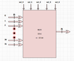
aa.png
 
Last edited:

Re: Question about a mltuiplexer based bus.

A 32x32 multiplexer will definitely consume "a lot of hardware" when it's implemented in FPGA. Your design description leaves no other choice than splitting it into many 4 or 6 input LUTs, whatever is available in the utilized FPGA family.

Looking at the mux implementation without considering the storage elements doesn't make much sense. An effective register file implementation will probably use FPGA block RAM, but it has restrictions regarding simultaneous storage access. Without knowing the intended memory function and all connections, it's impossible to determine if block RAM is an option.
 
Re: Question about a mltuiplexer based bus.

The error is likely due to an attempt to map to IO pins on the device. A 32 32:1 muxes isn't that bad for most devices. But 1056 IO pins is a bit much for most devices.

The design can also be implemented by using distributed memory. You can look at the synthesis manual to see coding styles that allow you to infer memories. DMEM is also nice for the 3x read, 1x read/write port configuration.
 
Re: Question about a mltuiplexer based bus.

A bash script to write this code? I can write the exact same code in <2 min.

if you are implementing this in a 6-input LUT architecture then you'll have 32x32 6-input LUTs just to select each bit of the bus before combining the 32 inputs into a single bit (using an additional 7 LUTs to do this) so I can see approximately 1248 LUTs, which will fit in any device I know of.

If you are using 4-input LUT architecture then I see something much larger...selecting each bit of the bus requires a 6-input LUT so you will have to break up the selection into multiple 4-input LUTs. The trade off in speed vs area would also affect the size of the circuit. It will likely consume about 1600 LUTs for the 4-input LUT version, which will fit in all but the smallest devices from generations back.

I think vGooditmes has pointed out the most likely error being the number of inputs and outputs. Use the don't insert I/O cells and the no trim options of the tools when implementing the design to implement it as a "core". Or if you can't figure out how to do that make a top level file with a shift register that connects to all the inputs/outputs of the mux module and connect the SDI/SDO, clock, and enable of the shift register to the pins isolating the mux from the pinout of the device.
 
Re: Question about a mltuiplexer based bus.

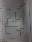
Yes I have made a TOP module and tested the design again, it was an IO problem. I was trying to implement something as shown in the picture from Morries Mano book but only with a 32 bit register file of 32 registers. Anyway I figured that I don't need the Mux since in a register file I will have a (read enable, write enable, read address and write address) is that right? I will however need the Mux as a bus if I am getting other inputs form else where right?

Also I will look into your suggestions. Thanks all are all awesome.

Sorry for the bad quality of the image.

11.jpg

- - - Updated - - -

@ads-ee
Use the don't insert I/O cells and the no trim options

How to do that in xilinx ISE?
 

Re: Question about a mltuiplexer based bus.

Right click on "Synthesize - XST" to bring up Process Properties - Xilinx Specific Options and turn off the -iobuf option.
Right click on "Implement Design" to bring up Process Properties - Map Properties and turn off -u (trim Unconnected signals)

That should allow you to run the tools all the way through Place & Route to get accurate timing and resource utilization.
 
Re: Question about a mltuiplexer based bus.

For modern Xilinx devices, I would think the resources would be closer to 256+16 = 272 LUTs. Each slice can implement a 16:1 mux by using the F7MUX and F8MUX. This gives 64 slices to get the first level of muxes. LUT6's can be configured to output two outputs from 5 common inputs, allowing a 2bit 2:1 mux per LUT -- 16 more slices.

For a register file, there would be 1024 registers. However the register to LUT ratio is at 2:1 on newer devices, so even that isn't bad.

Of course DMEM is a bit smaller as each slice can do 32x6bit, allowing this all to be done with 6 slices -- 24 LUT equivalents. Although the QuadPort (3x read, 1x read/write) at 32x2bit is probably the better choice. It would use 16 slices (64 LUT equivalent), but allows 3 registers to be read at the same time. This is very convenient. The Mano book probably doesn't make use of this, but it is of practical value if you ever need to implement a small processor.

If you need to have a register file + other inputs, it still makes sense to have the register file in DMEM and a small external mux for other registers.
 

Status
Not open for further replies.

Part and Inventory Search

Welcome to EDABoard.com

Sponsor

Back
Top