xiaoqianghit
Newbie
Hello, I have been using ADS simulation rectifier circuit in recent months. There are several problems that have been bothering me and I cannot continue. May I ask you for advice? Thanks a million!
Here I list three rectifier matching modules I made before. They are based on two kinds of plates, and each has its own emphasis in optimization direction during design. Good simulation results have been obtained in schematic simulation and co-simulation, but the measured results are not satisfactory.
Problem 1: inconsistency between co-simulation and test results
In each of the following three examples, this problem exists. The simulation results are good, but the measured results are mediocre or poor. Some need to deal with copper, can achieve satisfactory efficiency, some no matter how to adjust the efficiency and simulation efficiency is more than 20%.
I set the simulation mode as Momentum RFCosim mode in EM, and the simulation efficiency interval included 0Hz. Copper thickness and material characteristics were set in the plate settings.
Problem 2: S11 test results cannot reflect the matching effect
I used VNA to test the S11 and impedance of the rectifier matching module, and VNA was calibrated before the test. The results show that when a good S11 is tested, sometimes an acceptable efficiency is achieved (example 2 below) and sometimes it is not (example 3 below). My understanding is that since the output impedance of the VNA is 50Ω, when the rear stage achieves conjugate matching, it should also achieve reflection-free matching, and the S11 will also work best. But the actual results are different. S11 test results cannot reflect the matching effect.
The following are three matching cases of rectifier I made.
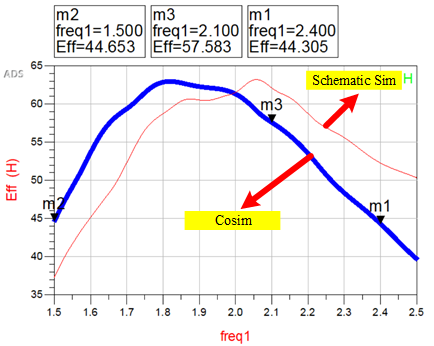
①A wide band (1.7GHz-2.1GHz) rectifier
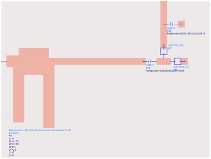
Based on ZYF255 plate processing, thickness 1.52mm, dielectric constant 2.55, loss factor 0.0018, using Schottky diode: SMS7630-079LF, the capacitor model is from murata official library.
Co-simulation:
Simulation results:
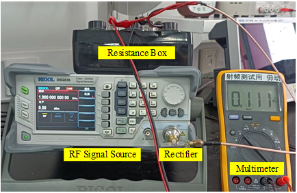
Efficiency test: (at 1.9GHz, 0dBm input, 1.6kΩ load, output voltage 0.111V, efficiency 0.77%)
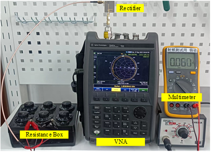
S11 test: (Input impedance 3.9+j*45.2Ω at 1.9GHz at 0dBm output)
②A 2.45GHz rectifier
Based on ZYF255 plate processing, thickness 1.52mm, dielectric constant 2.55, loss factor 0.0018, using Schottky diode: SMS7630-079LF, the capacitor model is from murata official library
Co-simulation:
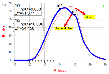
Simulation results:
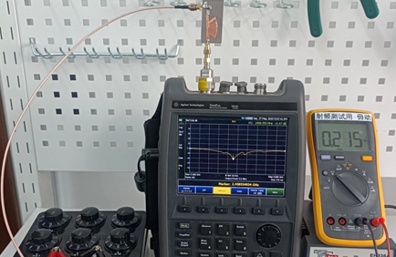
S11 test:(2.458GHz,-21.67dB)
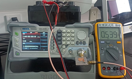
Efficiency test:(The highest voltage is 0.539V at 2.44GHz, and the efficiency is 29% at 0dBm and 1kΩ load)
③A 2.45GHz rectifier
Based on FR4 plate machining, thickness 1.6mm, dielectric constant 4.4, loss factor 0.02, using Schottky diode: SMS7630-079LF, using capacitance model from murata official library
Co-simulation:
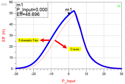
Simulation results:
S11 test:(2.557GHz,-24.22dB)
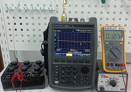
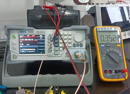
Efficiency measurement: (2.557GHz, 1kΩ load, output voltage 0.352V, efficiency 12.4%)
Here I list three rectifier matching modules I made before. They are based on two kinds of plates, and each has its own emphasis in optimization direction during design. Good simulation results have been obtained in schematic simulation and co-simulation, but the measured results are not satisfactory.
Problem 1: inconsistency between co-simulation and test results
In each of the following three examples, this problem exists. The simulation results are good, but the measured results are mediocre or poor. Some need to deal with copper, can achieve satisfactory efficiency, some no matter how to adjust the efficiency and simulation efficiency is more than 20%.
I set the simulation mode as Momentum RFCosim mode in EM, and the simulation efficiency interval included 0Hz. Copper thickness and material characteristics were set in the plate settings.
Problem 2: S11 test results cannot reflect the matching effect
I used VNA to test the S11 and impedance of the rectifier matching module, and VNA was calibrated before the test. The results show that when a good S11 is tested, sometimes an acceptable efficiency is achieved (example 2 below) and sometimes it is not (example 3 below). My understanding is that since the output impedance of the VNA is 50Ω, when the rear stage achieves conjugate matching, it should also achieve reflection-free matching, and the S11 will also work best. But the actual results are different. S11 test results cannot reflect the matching effect.
The following are three matching cases of rectifier I made.
①A wide band (1.7GHz-2.1GHz) rectifier
Based on ZYF255 plate processing, thickness 1.52mm, dielectric constant 2.55, loss factor 0.0018, using Schottky diode: SMS7630-079LF, the capacitor model is from murata official library.
Co-simulation:
Simulation results:
Efficiency test: (at 1.9GHz, 0dBm input, 1.6kΩ load, output voltage 0.111V, efficiency 0.77%)
S11 test: (Input impedance 3.9+j*45.2Ω at 1.9GHz at 0dBm output)
②A 2.45GHz rectifier
Based on ZYF255 plate processing, thickness 1.52mm, dielectric constant 2.55, loss factor 0.0018, using Schottky diode: SMS7630-079LF, the capacitor model is from murata official library
Co-simulation:
Simulation results:
S11 test:(2.458GHz,-21.67dB)
Efficiency test:(The highest voltage is 0.539V at 2.44GHz, and the efficiency is 29% at 0dBm and 1kΩ load)
③A 2.45GHz rectifier
Based on FR4 plate machining, thickness 1.6mm, dielectric constant 4.4, loss factor 0.02, using Schottky diode: SMS7630-079LF, using capacitance model from murata official library
Co-simulation:
Simulation results:
S11 test:(2.557GHz,-24.22dB)
Efficiency measurement: (2.557GHz, 1kΩ load, output voltage 0.352V, efficiency 12.4%)