Continue to Site

Welcome to EDAboard.com

Welcome to our site! EDAboard.com is an international Electronics Discussion Forum focused on EDA software, circuits, schematics, books, theory, papers, asic, pld, 8051, DSP, Network, RF, Analog Design, PCB, Service Manuals... and a whole lot more! To participate you need to register. Registration is free. Click here to register now.

problem with LDO design!

Status
Not open for further replies.
congrats dear you have done it!!

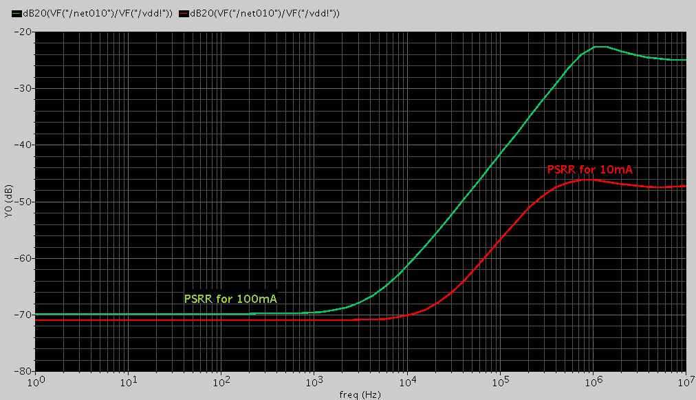
but did u notice the difference between two values of psrr at dc freqs ...

I asked u to run sim for 100mA just for that ... this will provide u some insight in psr behaviour of ldo.
 

i inderstand now why to run these tow simulations!

so the PSRR decreses if the the load current increase, also the deep in the PSRR changes.

the rejection is better with low load current

you will find joined the comparaison of the two simulations:


thanks !

regards.
 

Hi imar,

I think your results look rather good.
One further question: I suppose during PSSR ac simulation the input voltage plus ac signal was applied also (as a supply) to the error amplifier, is this true ?
Regards
 

Hi LvW!
yes, the input voltage with ac component was applied to the error amplifier as a supply voltage.

regards!
 

Hi again!!

i have two main questions:

* how can i manage to simulate the noise generated by the LDO ? and is it so important to evaluate it especially i think that this noise is mostly generated by the bandgap?

* concerning the layout implimentation, should the bandgap be integrated all the time in the same chip that contains the other parts of the LDO? for me i think it is yes to reduce the length of path that connect them!

thanks for responses !
regards
 

Hi Imar,

1) You can simulate the noise performance of your LDO by using ".noise" command in hspice... or simply setup noise analysis option in ur simulator (probably spectre).

Yes u are right that band-gap is a major contributor to LDO noise... for this u can refer to "analog applications journal" from TI... it gives a good idea .

2)Yes mostly the band-gap is integrated onthe same chip as LDO... taking care of its placement with respect to the pass device...(BGR should be far from pass device to take care of temprature drift).

hope this helps
 

thanks Ashish-chauhan!

* concerning the noise simulation, i am using spectre and not Hspice!

*concerning the BNG integrartion in same chip that contains the LDO, there is a point that i found not clear : the input voltage of this BNG which is, i think, vdd should be stable, or when doing the line regulation the vdd changes.

so how can i manage to fixe the input voltage of the BNG? could it be an extra voltage source or the output voltage of the LDO.

note: when simulating the LDO, i used a Vdc voltage that generates 1.2V to replace the bandgap. and now i am trying to replace this ideal voltage source by a bandgap that was already prepared.

what should i do to solve this problem!

thanks.
 

Hi

Well the vdd for bgr is generally the same as that of LDO , that is the unregulated supply... this so becoz on full chips there are circuits like POR and BOR which might use bgr o/p even when ldo o/p is not present /stable.

In most cases the bgr is designed to have good psrr so that it does not get affected with supply noise... and as far as vdd variation is concerned the bangap output is quite insensitive to that...

Still there are structures where bgr itself is supplied from ldo output...
It depends on ur specs...
 

You need to specify the max an d min supply voltage and load current then size the pass device to be in saturation for min dropout and max current. That way you limit gain variations and achieve stability for worst case which can be max or min depending on comp scheme
 

hi !
ashish_chauhan said:
Hi

Still there are structures where bgr itself is supplied from ldo output...
It depends on ur specs...

in this case i think i might use a start up circuit.
**************

i have a general question that comes in mind and it has no relation with that problem: if i would transform my LDO to a simple linear regulator that generates let's say for exemple 1.2V in steed of 2.8V ( when acting as LDO), what should i do?
is there any changes that affect the LDO architecture to allow the high drop out voltage (3.3V as input - 1.2 V as output = 2.1V)?

thanks
 

Hi Imar,

Well first change I would do (assuming I have sufficient headroom for all the input vdds) is to replace pmos with nmos ... this will ease off my compensation scheme.
And my dependence on output cap for stability will be relaxed. The pass device size will be small(being nmos) and so shall be the parasitic cap at gate of pass device.

typically if you have a drop out of 500mv ... u can go for noms device instead of pmos...

hope this answers ur question.

as of first question... yes u will need a startup circuit
( bgr usually has one implemented with it).
 

hi Ashich_chauhan!

ashish_chauhan said:
Well first change I would do (assuming I have sufficient headroom for all the input vdds) is to replace pmos with nmos ... . The pass device size will be small(being nmos) and so shall be the parasitic cap at gate of pass device.

typically if you have a drop out of 500mv ... u can go for noms device instead of pmos...
[/u]

i am really sorry but i want to learn more, can you explain me how to replace the PMOS with a NMOS? it is a new issue that i am in front of!!
should i connect the drain to vdd directly or what?

concerning the size if the pass element, tou said that i will be small!
let's take an example, for a dropout voltage of 0.5V, w/l =10000of the PMOS igives acceptable results.
for the NMOS, what will be the expression of Vdrop out and for a current of 60mA , what will be theoretically the w/l ratio?

thanks in advance!
 

Yes u will connect drain to vdd directly... and take out put at source... that way ur o/p stage becomes a source follower...

talking of size... just try to simulate a pmos and nmos for similar current capacities
u will see the difference.

theoritically just apply the saturation region current equation to nmos and calculate the sizes... and expression for vdropout is always vd=vin-vout;
drop out occurs when regulators stops regulating and vds of device strats changing as curent demand changes.

hope i made myself clear ...
 

Status
Not open for further replies.

Similar threads

Part and Inventory Search

Welcome to EDABoard.com

Sponsor

Back
Top