Continue to Site

Welcome to EDAboard.com

Welcome to our site! EDAboard.com is an international Electronics Discussion Forum focused on EDA software, circuits, schematics, books, theory, papers, asic, pld, 8051, DSP, Network, RF, Analog Design, PCB, Service Manuals... and a whole lot more! To participate you need to register. Registration is free. Click here to register now.

Problem about output buffer for DAC

Status
Not open for further replies.

afujian

Member level 4
Joined
Mar 26, 2010
Messages
70
Helped
2
Reputation
4
Reaction score
1
Trophy points
1,288
Location
china
Activity points
1,715
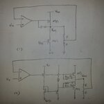
Hi all,I'm designing a output buffer for DAC, and intend to use a 2 stage miller compensated OP or a OP with class-AB output stage as showed in the picture(1) and (2),they are both feedback connected by 2 equal resistors to get a X2 gain,but the simulation show that when the input voltage changes from 0 to 1mV,the output node Vout changes very slow while the target settling time is about 2uS,when the input changes from 1V-1.001V,the output changes normally.I think this is because when the voltage of node Vout is very low,the whole loop doesn't work,so is there any way to solve the probelm? Thanks a lot.
20130121_095753.jpg
Simulation results
Tran.JPG
 

When the input is 0 mV, are all the transistors in saturation? Do you have a nMOS+pMOS input pair? I think the signs of the first stage written in the diagram are wrong.
 

Which opamp are you using, and what is it's power supply -- is it dual/ split or single ?

I think opamps do not work very well with inputs near GND for single supply OP's ? This might be where the problem lies.
 

Additional, one important question, in your OP (the triangle symbol) is that just a differential pair, thus a single stage? I only bring this up because diagram (1) is a two stage when including the output stage (all like Rakshitdatta) the minus terminal should be swapped. You have positive feedback now. And in diagram (2) you have a three stage nested-miller amplifier, therefore you need to make sure to compensate that correctly. It isn't just Cc1=Cc2 and Rc1=Rc2. That only works when having stage2 = 3*GBW and stage3=5*GBW which is a waste of power....

JGK
 

Thanks rakshitdatta,you remind me,I'm sorry for the confusion,when I write the sign I mean it is for the whole op not just the first stage.There is only Pmos input pair.

- - - Updated - - -

Which opamp are you using, and what is it's power supply -- is it dual/ split or single ?

I think opamps do not work very well with inputs near GND for single supply OP's ? This might be where the problem lies.

I intend to use both of them to configure the output buffer with fast mode(picture(1)) and slow mode(picture(2)),the power supply is single,as the op will not work well when the input near GND, should I ignore the output error when DAC code equal or near zero(the DAC is R-string structre).

- - - Updated - - -

Additional, one important question, in your OP (the triangle symbol) is that just a differential pair, thus a single stage? I only bring this up because diagram (1) is a two stage when including the output stage (all like Rakshitdatta) the minus terminal should be swapped. You have positive feedback now. And in diagram (2) you have a three stage nested-miller amplifier, therefore you need to make sure to compensate that correctly. It isn't just Cc1=Cc2 and Rc1=Rc2. That only works when having stage2 = 3*GBW and stage3=5*GBW which is a waste of power....

JGK

The signs should be swapped,The OP in the triangle is a simple differential input(or folded cascode structre),because of the project requirement,both of the op will be used,thanks for your remind for the op design.
 

Status
Not open for further replies.

Part and Inventory Search

Welcome to EDABoard.com

Sponsor

Back
Top