Continue to Site

Welcome to EDAboard.com

Welcome to our site! EDAboard.com is an international Electronics Discussion Forum focused on EDA software, circuits, schematics, books, theory, papers, asic, pld, 8051, DSP, Network, RF, Analog Design, PCB, Service Manuals... and a whole lot more! To participate you need to register. Registration is free. Click here to register now.

Power switches/mosfets please help

Status
Not open for further replies.
Yeah, I didn't check it but I'm sure it's probably just a square wave.

If anyone is interested...

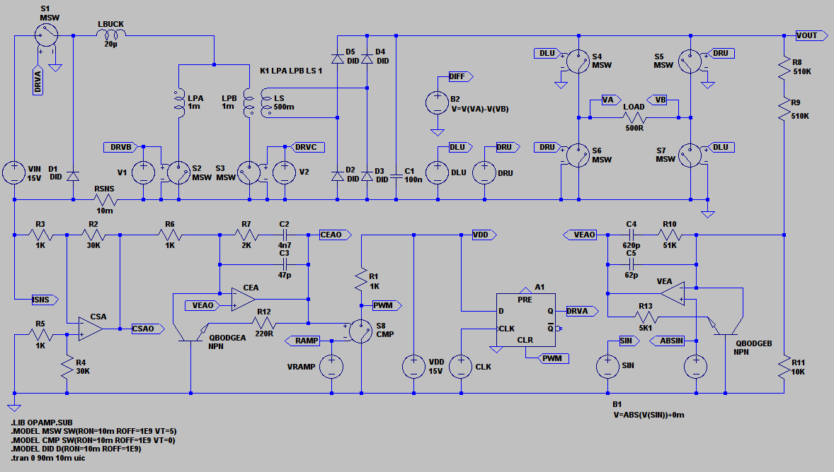
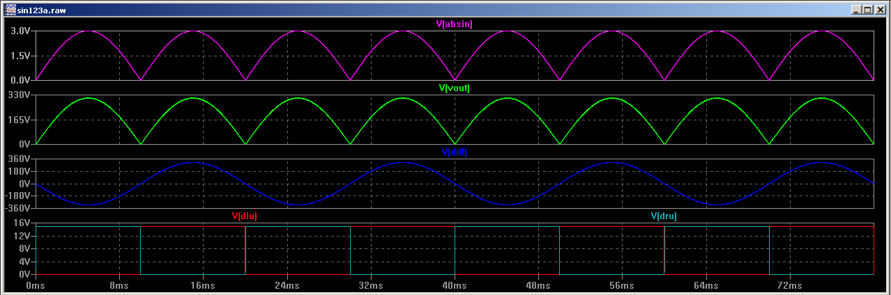
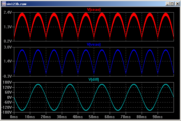
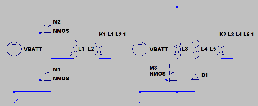
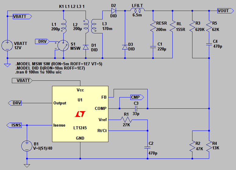
Upon further research, it seems like the most common method is to use a push-pull topology to convert the 12VDC to 12VAC at high frequency, use a hf transformer to step-up to ~110VAC, then rectify to ~180VDC. Then this is inverted using H-bridge to 110VAC at 60Hz. Also, a LPF is used either after the rectification or the H-bridge to get a sine. So the high frequency operation is in the front-end to step up the input voltage. Later, in the H-bridge the desired output frequency (50/60Hz) is used. Otherwise, a large transformer is needed if not using a high frequency front-end.
 

Have a look at,

https://www.edaboard.com/threads/202321/#post855461

I'll reproduce it here..


This is based on the UC3827

https://focus.ti.com/lit/ds/symlink/uc3827-1.pdf
**broken link removed**

It 'looks' complex and in some respects I suppose it is. However all the control at the bottom is contained within the IC.

What you will need is a sine generator and precision active rectifier. Might just be a couple of quad op-amps. As you have noted there is the push-pull transformer with switches.

There is the penalty of the extra buck switch/mosfet on the primary but you do not need the output filter inductor.

All the sine generation is done on the primary side. As far as the bridge is concerned you do not have to 'PWM' it to get the sine wave out. You just 'chop' it at the required 50/60Hz output frequency.

Hopefully the following waveforms make sense. Do you have LTSPice?


Genome.
 

This is the output of the above circuit?

The schematic is almost too sophisticated for me. I do have LT Spice. If you have the files for LT Spice can you please provide them to me so I can play with your circuit? Is that how you simulate a transformer in LT Spice?

This is based on the UC3827

So all the labeled signals in the schematic are coming from a UC3827, signals which you have simulated?

Thanks!
 

It probably is 'sophisticated' but it is the best way I can think of coming up with a 'pure sine wave'. Perhaps it looks complicated but as suggested much of the control is buried in the UC3827.

Not all of the signals come from it. Just the drive and control for the primary side switches. You will still need to generate the sine/half sine and the 50/60Hz drive for the secondary side bridge.

That's how I model 'ideal' transformers' in spice. Coupled inductors with values set as inductances according to squares of turns ratios.

Here is the model.. I've just realised I have done silly things elsewhere.

Code:
Version 4
SHEET 1 1448 1312
WIRE -816 -64 -864 -64
WIRE -704 -64 -736 -64
WIRE -640 -64 -704 -64
WIRE -320 -64 -560 -64
WIRE 96 -64 16 -64
WIRE 176 -64 96 -64
WIRE 672 -64 176 -64
WIRE 976 -64 672 -64
WIRE 1232 -64 976 -64
WIRE 1264 -64 1232 -64
WIRE 16 -32 16 -64
WIRE 96 -32 96 -64
WIRE 672 -32 672 -64
WIRE 976 -32 976 -64
WIRE 1232 -16 1232 -64
WIRE -800 16 -800 -16
WIRE -752 16 -752 -16
WIRE -320 16 -320 -64
WIRE -320 16 -416 16
WIRE -224 16 -320 16
WIRE 320 48 288 48
WIRE 624 64 624 32
WIRE 1024 64 1024 32
WIRE -416 80 -416 16
WIRE -224 80 -224 16
WIRE 96 80 96 32
WIRE 96 80 -176 80
WIRE 288 80 288 48
WIRE 1232 96 1232 64
WIRE 736 112 704 112
WIRE 944 112 912 112
WIRE 16 160 16 32
WIRE 16 160 -176 160
WIRE 672 160 672 48
WIRE 704 160 704 112
WIRE 704 160 672 160
WIRE 784 160 704 160
WIRE 944 160 944 112
WIRE 944 160 864 160
WIRE 976 160 976 48
WIRE 976 160 944 160
WIRE 288 192 288 160
WIRE 672 224 672 160
WIRE 976 224 976 160
WIRE -512 240 -528 240
WIRE -464 240 -512 240
WIRE -128 240 -176 240
WIRE -112 240 -128 240
WIRE 320 240 288 240
WIRE 448 240 416 240
WIRE -864 272 -864 -64
WIRE -512 272 -512 240
WIRE -416 272 -416 160
WIRE -224 272 -224 160
WIRE -128 272 -128 240
WIRE 288 272 288 240
WIRE 416 272 416 240
WIRE -704 288 -704 -64
WIRE -464 288 -464 240
WIRE -176 288 -176 240
WIRE 16 288 16 160
WIRE 96 288 96 80
WIRE 176 288 176 -64
WIRE -864 384 -864 352
WIRE -704 384 -704 352
WIRE -704 384 -864 384
WIRE -656 384 -704 384
WIRE -512 384 -512 352
WIRE -512 384 -576 384
WIRE -464 384 -464 336
WIRE -464 384 -512 384
WIRE -416 384 -416 352
WIRE -416 384 -464 384
WIRE -224 384 -224 352
WIRE -224 384 -416 384
WIRE -176 384 -176 336
WIRE -176 384 -224 384
WIRE -128 384 -128 352
WIRE -128 384 -176 384
WIRE 16 384 16 352
WIRE 16 384 -128 384
WIRE 96 384 96 352
WIRE 96 384 16 384
WIRE 176 384 176 352
WIRE 176 384 96 384
WIRE 288 384 288 352
WIRE 288 384 176 384
WIRE 416 384 416 352
WIRE 416 384 288 384
WIRE 624 384 624 288
WIRE 624 384 416 384
WIRE 672 384 672 304
WIRE 672 384 624 384
WIRE 976 384 976 304
WIRE 976 384 672 384
WIRE 1024 384 1024 288
WIRE 1024 384 976 384
WIRE 1024 416 1024 384
WIRE -864 480 -864 384
WIRE -832 480 -864 480
WIRE -720 480 -752 480
WIRE -688 480 -720 480
WIRE -576 480 -608 480
WIRE -480 480 -576 480
WIRE -304 480 -400 480
WIRE -272 480 -304 480
WIRE -160 480 -192 480
WIRE -64 480 -96 480
WIRE -32 480 -64 480
WIRE 224 480 80 480
WIRE 352 480 224 480
WIRE 384 480 352 480
WIRE 752 480 720 480
WIRE 784 480 752 480
WIRE 880 480 848 480
WIRE 992 480 960 480
WIRE 1232 480 1232 176
WIRE 1232 480 992 480
WIRE -304 560 -304 480
WIRE -160 560 -304 560
WIRE -64 560 -64 480
WIRE -64 560 -96 560
WIRE 80 560 80 480
WIRE 752 560 752 480
WIRE 784 560 752 560
WIRE 992 560 992 480
WIRE 992 560 848 560
WIRE 992 624 992 560
WIRE 992 624 960 624
WIRE 1120 624 992 624
WIRE -304 640 -304 560
WIRE -304 640 -432 640
WIRE -272 640 -304 640
WIRE 752 640 752 560
WIRE 896 640 752 640
WIRE -864 656 -864 480
WIRE -816 656 -864 656
WIRE -64 656 -64 560
WIRE -64 656 -208 656
WIRE 992 656 960 656
WIRE -272 672 -304 672
WIRE 80 672 80 640
WIRE 112 672 80 672
WIRE 352 688 352 480
WIRE 448 688 352 688
WIRE 640 688 608 688
WIRE 80 704 80 672
WIRE 752 704 752 640
WIRE 816 704 752 704
WIRE 1024 704 896 704
WIRE 1120 704 1120 624
WIRE -720 720 -720 480
WIRE -688 720 -720 720
WIRE -432 720 -432 640
WIRE -224 720 -336 720
WIRE -64 720 -64 656
WIRE -64 720 -144 720
WIRE 32 720 -64 720
WIRE -576 736 -576 480
WIRE -576 736 -624 736
WIRE -544 736 -576 736
WIRE 448 736 352 736
WIRE -832 752 -864 752
WIRE -720 752 -752 752
WIRE -688 752 -720 752
WIRE 0 768 -32 768
WIRE 32 768 0 768
WIRE 784 768 752 768
WIRE 992 768 992 656
WIRE 992 768 960 768
WIRE -720 800 -720 752
WIRE 0 800 0 768
WIRE 224 800 224 480
WIRE 352 800 352 736
WIRE 752 800 752 768
WIRE 992 800 992 768
WIRE 1232 800 1232 480
WIRE 528 816 528 784
WIRE 560 816 528 816
WIRE -864 912 -864 752
WIRE -720 912 -720 880
WIRE -720 912 -864 912
WIRE -384 912 -384 784
WIRE -384 912 -720 912
WIRE 0 912 0 880
WIRE 0 912 -384 912
WIRE 80 912 80 784
WIRE 80 912 0 912
WIRE 224 912 224 880
WIRE 224 912 80 912
WIRE 352 912 352 880
WIRE 352 912 224 912
WIRE 752 912 752 880
WIRE 752 912 352 912
WIRE 992 912 992 880
WIRE 992 912 752 912
WIRE 1072 912 1072 768
WIRE 1072 912 992 912
WIRE 1232 912 1232 880
WIRE 1232 912 1072 912
WIRE -864 944 -864 912
FLAG -528 240 DRVB
IOPIN -528 240 In
FLAG -112 240 DRVC
IOPIN -112 240 In
FLAG -752 16 0
FLAG -800 16 DRVA
IOPIN -800 16 In
FLAG 1024 416 0
FLAG -816 656 ISNS
IOPIN -816 656 Out
FLAG 624 64 0
FLAG 1024 64 0
FLAG 736 112 VA
IOPIN 736 112 Out
FLAG 912 112 VB
IOPIN 912 112 Out
FLAG 1264 -64 VOUT
IOPIN 1264 -64 Out
FLAG 112 672 PWM
IOPIN 112 672 Out
FLAG 528 640 0
FLAG 448 784 0
FLAG 560 816 PWM
IOPIN 560 816 In
FLAG 640 688 DRVA
IOPIN 640 688 Out
FLAG -864 944 0
FLAG -32 768 RAMP
IOPIN -32 768 Out
FLAG 384 480 VDD
IOPIN 384 480 Out
FLAG -32 480 CEAO
IOPIN -32 480 Out
FLAG -544 736 CSAO
IOPIN -544 736 Out
FLAG -304 672 VEAO
IOPIN -304 672 In
FLAG 720 480 VEAO
IOPIN 720 480 Out
FLAG 784 768 SIN
IOPIN 784 768 Out
FLAG 960 768 ABSIN
IOPIN 960 768 Out
FLAG 320 240 DLU
IOPIN 320 240 Out
FLAG 448 240 DRU
IOPIN 448 240 Out
FLAG 624 -16 DLU
IOPIN 624 -16 In
FLAG 1024 240 DLU
IOPIN 1024 240 In
FLAG 624 240 DRU
IOPIN 624 240 In
FLAG 1024 -16 DRU
IOPIN 1024 -16 In
FLAG 288 192 0
FLAG 320 48 DIFF
IOPIN 320 48 Out
SYMBOL ind2 -432 176 M180
WINDOW 0 42 68 Left 0
WINDOW 3 42 46 Left 0
SYMATTR InstName LPA
SYMATTR Value 55�
SYMATTR Type ind
SYMBOL ind2 -208 64 M0
WINDOW 0 49 44 Left 0
WINDOW 3 57 66 Left 0
SYMATTR InstName LPB
SYMATTR Value 55�
SYMATTR Type ind
SYMBOL ind -656 -48 R270
WINDOW 0 32 56 VTop 0
WINDOW 3 5 56 VBottom 0
SYMATTR InstName LBUCK
SYMATTR Value 2.5�
SYMBOL sw -720 -64 M270
WINDOW 0 73 71 VLeft 0
WINDOW 3 48 72 VLeft 0
SYMATTR InstName S1
SYMATTR Value MSW
SYMBOL diode -688 352 R180
WINDOW 0 55 51 Left 0
WINDOW 3 44 30 Left 0
SYMATTR InstName D1
SYMATTR Value DID
SYMBOL sw -416 368 M180
WINDOW 0 38 69 Left 0
WINDOW 3 38 45 Left 0
SYMATTR InstName S2
SYMATTR Value MSW
SYMBOL sw -224 368 R180
WINDOW 0 65 69 Left 0
WINDOW 3 37 45 Left 0
SYMATTR InstName S3
SYMATTR Value MSW
SYMBOL ind2 -160 64 M0
WINDOW 0 -33 44 Left 0
WINDOW 3 -81 67 Left 0
SYMATTR InstName LS
SYMATTR Value 26.7m
SYMATTR Type ind
SYMBOL diode 32 352 R180
WINDOW 0 -34 49 Left 0
WINDOW 3 -45 24 Left 0
SYMATTR InstName D2
SYMATTR Value DID
SYMBOL diode 112 352 R180
WINDOW 0 -33 46 Left 0
WINDOW 3 -43 22 Left 0
SYMATTR InstName D3
SYMATTR Value DID
SYMBOL diode 112 32 R180
WINDOW 0 -35 51 Left 0
WINDOW 3 -45 26 Left 0
SYMATTR InstName D4
SYMATTR Value DID
SYMBOL diode 32 32 R180
WINDOW 0 -33 52 Left 0
WINDOW 3 -45 27 Left 0
SYMATTR InstName D5
SYMATTR Value DID
SYMBOL cap 160 288 R0
WINDOW 0 41 19 Left 0
WINDOW 3 40 42 Left 0
SYMATTR InstName C1
SYMATTR Value 100n
SYMBOL voltage -864 256 R0
WINDOW 0 40 45 Left 0
WINDOW 3 37 69 Left 0
SYMATTR InstName VIN
SYMATTR Value 12V
SYMBOL voltage -512 256 R0
WINDOW 0 -71 55 Left 0
WINDOW 3 24 104 Invisible 0
WINDOW 123 0 0 Left 0
WINDOW 39 0 0 Left 0
SYMATTR InstName V1
SYMATTR Value PULSE(0 15 0 10n 10n 5.25u 10u)
SYMBOL voltage -128 256 R0
WINDOW 0 41 52 Left 0
WINDOW 3 24 104 Invisible 0
WINDOW 123 0 0 Left 0
WINDOW 39 0 0 Left 0
SYMATTR InstName V2
SYMATTR Value PULSE(0 15 5u 10n 10n 5.25u 10u)
SYMBOL res -560 368 R90
WINDOW 0 0 56 VBottom 0
WINDOW 3 32 56 VTop 0
SYMATTR InstName RSNS
SYMATTR Value 3m
SYMBOL sw 672 64 M180
WINDOW 0 39 69 Left 0
WINDOW 3 39 47 Left 0
SYMATTR InstName S4
SYMATTR Value MSW
SYMBOL sw 976 64 R180
WINDOW 0 71 70 Left 0
WINDOW 3 45 47 Left 0
SYMATTR InstName S5
SYMATTR Value MSW
SYMBOL sw 672 320 M180
WINDOW 0 39 69 Left 0
WINDOW 3 39 45 Left 0
SYMATTR InstName S6
SYMATTR Value MSW
SYMBOL sw 976 320 R180
WINDOW 0 65 69 Left 0
WINDOW 3 40 46 Left 0
SYMATTR InstName S7
SYMATTR Value MSW
SYMBOL voltage 0 784 R0
WINDOW 0 -120 57 Left 0
WINDOW 3 24 104 Invisible 0
WINDOW 123 0 0 Left 0
WINDOW 39 0 0 Left 0
SYMATTR InstName VRAMP
SYMATTR Value PULSE(0.5 2.9 0 4.5u 500n 0 5u)
SYMBOL sw 80 800 M180
WINDOW 0 43 72 Left 0
WINDOW 3 43 48 Left 0
SYMATTR InstName S8
SYMATTR Value CMP
SYMBOL res 64 544 R0
WINDOW 0 40 49 Left 0
WINDOW 3 41 76 Left 0
SYMATTR InstName R1
SYMATTR Value 1K
SYMBOL Digital\\dflop 528 640 R0
WINDOW 0 27 -18 Left 0
SYMATTR InstName A1
SYMATTR SpiceLine Vhigh=15 Vlow=0 Td=10n
SYMBOL voltage 352 784 R0
WINDOW 0 41 56 Left 0
WINDOW 3 24 104 Invisible 0
WINDOW 123 0 0 Left 0
WINDOW 39 0 0 Left 0
SYMATTR InstName CLK
SYMATTR Value PULSE(0 15 0 10n 10n 1u 5u)
SYMBOL voltage 224 784 R0
WINDOW 0 41 42 Left 0
WINDOW 3 41 68 Left 0
WINDOW 123 0 0 Left 0
WINDOW 39 0 0 Left 0
SYMATTR InstName VDD
SYMATTR Value 15V
SYMBOL Opamps\\opamp -656 672 R0
SYMATTR InstName CSA
SYMATTR SpiceLine2 GBW=100Meg
SYMBOL res -592 464 R90
WINDOW 0 0 56 VBottom 0
WINDOW 3 32 56 VTop 0
SYMATTR InstName R2
SYMATTR Value 15K
SYMBOL res -736 464 R90
WINDOW 0 0 56 VBottom 0
WINDOW 3 32 56 VTop 0
SYMATTR InstName R3
SYMATTR Value 1K
SYMBOL res -736 784 R0
WINDOW 0 42 44 Left 0
WINDOW 3 43 67 Left 0
SYMATTR InstName R4
SYMATTR Value 15K
SYMBOL res -736 736 R90
WINDOW 0 0 56 VBottom 0
WINDOW 3 32 56 VTop 0
SYMATTR InstName R5
SYMATTR Value 1K
SYMBOL Opamps\\opamp -240 592 R0
SYMATTR InstName CEA
SYMATTR SpiceLine2 GBW=100Meg
SYMBOL res -384 464 R90
WINDOW 0 0 56 VBottom 0
WINDOW 3 32 56 VTop 0
SYMATTR InstName R6
SYMATTR Value 2K
SYMBOL res -176 464 R90
WINDOW 0 0 56 VBottom 0
WINDOW 3 32 56 VTop 0
SYMATTR InstName R7
SYMATTR Value 3K
SYMBOL cap -96 464 R90
WINDOW 0 0 32 VBottom 0
WINDOW 3 32 32 VTop 0
SYMATTR InstName C2
SYMATTR Value 3n3
SYMBOL cap -96 544 R90
WINDOW 0 0 32 VBottom 0
WINDOW 3 32 32 VTop 0
SYMATTR InstName C3
SYMATTR Value 47p
SYMBOL Opamps\\opamp 928 576 M0
SYMATTR InstName VEA
SYMATTR SpiceLine2 GBW=100Meg
SYMBOL res 1216 -32 R0
WINDOW 0 40 42 Left 0
WINDOW 3 42 67 Left 0
SYMATTR InstName R8
SYMATTR Value 510K
SYMBOL res 1216 80 R0
SYMATTR InstName R9
SYMATTR Value 510K
SYMBOL bv 992 784 R0
WINDOW 0 -226 159 Left 0
WINDOW 3 -224 187 Left 0
SYMATTR InstName B1
SYMATTR Value V=ABS(V(SIN))+10m
SYMBOL res 976 464 R90
WINDOW 0 0 56 VBottom 0
WINDOW 3 32 56 VTop 0
SYMATTR InstName R10
SYMATTR Value 51K
SYMBOL cap 848 464 R90
WINDOW 0 0 32 VBottom 0
WINDOW 3 32 32 VTop 0
SYMATTR InstName C4
SYMATTR Value 620p
SYMBOL cap 848 544 R90
WINDOW 0 0 32 VBottom 0
WINDOW 3 32 32 VTop 0
SYMATTR InstName C5
SYMATTR Value 62p
SYMBOL voltage 752 784 R0
WINDOW 0 39 53 Left 0
WINDOW 3 24 104 Invisible 0
WINDOW 123 0 0 Left 0
WINDOW 39 0 0 Left 0
SYMATTR InstName SIN
SYMATTR Value SINE(0 3 50 0)
SYMBOL res 1216 784 R0
WINDOW 0 38 45 Left 0
WINDOW 3 37 70 Left 0
SYMATTR InstName R11
SYMATTR Value 20K
SYMBOL voltage 288 256 R0
WINDOW 0 39 55 Left 0
WINDOW 3 24 104 Invisible 0
WINDOW 123 0 0 Left 0
WINDOW 39 0 0 Left 0
SYMATTR InstName DLU
SYMATTR Value PULSE(0 15 0 10n 10n 9.99m 20m)
SYMBOL voltage 416 256 R0
WINDOW 0 39 57 Left 0
WINDOW 3 24 104 Invisible 0
WINDOW 123 0 0 Left 0
WINDOW 39 0 0 Left 0
SYMATTR InstName DRU
SYMATTR Value PULSE(0 15 10m 10n 10n 9.99m 20m)
SYMBOL res 880 144 R90
WINDOW 0 0 56 VBottom 0
WINDOW 3 32 56 VTop 0
SYMATTR InstName LOAD
SYMATTR Value 60R5
SYMBOL bv 288 64 R0
WINDOW 0 38 46 Left 0
WINDOW 3 40 73 Left 0
SYMATTR InstName B2
SYMATTR Value V=V(VA)-V(VB)
SYMBOL npn -432 784 R270
WINDOW 0 22 100 VRight 0
WINDOW 3 0 99 VRight 0
SYMATTR InstName QBODGEA
SYMBOL npn 1120 768 M270
WINDOW 0 -8 -80 VRight 0
WINDOW 3 -31 -16 VRight 0
SYMATTR InstName QBODGEB
SYMBOL res -128 704 R90
WINDOW 0 0 56 VBottom 0
WINDOW 3 32 56 VTop 0
SYMATTR InstName R12
SYMATTR Value 10R
SYMBOL res 912 688 R90
WINDOW 0 0 56 VBottom 0
WINDOW 3 32 56 VTop 0
SYMATTR InstName R13
SYMATTR Value 10R
TEXT -192 32 Left 0 !K1 LPA LPB LS 1
TEXT -872 1016 Left 0 !.MODEL MSW SW(RON=3m ROFF=1E9 VT=5)
TEXT -872 1064 Left 0 !.MODEL DID D(RON=10m ROFF=1E9)
TEXT -872 1088 Left 0 !.tran 0 110m 10m uic
TEXT -872 992 Left 0 !.LIB OPAMP.SUB
TEXT -872 1040 Left 0 !.MODEL CMP SW(RON=10m ROFF=1E9 VT=0)

copy the text into your text editor and save it as a .asc file.

Be afraid... as FvM has suggested you get some 'wicked' currents flying about especially if you want 200W from 12V

Genome.
 
There seems to be something wrong with the control loop polarity. I also don't get the purpose of summing current and voltage process values. If a current limiting action is intended, there should be a kind of analog "OR" respectively max() operation.

Why don't you simply post a zipped *.asc file?
 
This is 'average current mode control'. There is an internal current loop that sets the primary side inductor current which gets reflected through to the secondary by the push-pull stage and transformer. Effectively it is a buck converter but the transformer provides for step up. The voltage loop sets the current demand for the current loop. There is an internal peak current limit within the UC3827 otherwise it is possible to limit the output of the voltage error amplifier to achieve a similar function which might be preferable.

The loop polarity is correct, at least for the model and I do believe it matches what the UC3827 implements, but being what it is it is 'hard' to follow things through.

Why don't you simply post a zipped *.asc file?

Thanks.. just worked out how to do it.

Genome.
 

Attachments

  • sin123a.zip
    2.9 KB · Views: 74
I didn't analyze the circuit, but saw the controller output wind-up to kV and MV while the buck converter stays off when running your analysis setup. Of course, there may be other reasons for the behaviour as well, e.g. missing voltage limitation for the integrator that the real device has.

I understand know, that the current control loop is simply representing UC38xx current mode, I didn't think about it sufficiently.

Downloads.. Quick/Slow check.. As delivered it does what it says on the 'tin'.


You've been having a 'play', haven't you.

Genome.
 
Genome, thanks! I had a hang up but I'm back at it. Just downloaded your circuit and I'm going to take a look at it.
 

Downloads.. Quick/Slow check.. As delivered it does what it says on the 'tin'.
Yes, everythink O.K. Unfortunately I have been simulating the text from the code window before you managed to provided a zip file. It has a few "µ" symbols replaced by "?".
 
Genome, your circuit is pretty awesome. I really only need a modified sine, and I understand the H-bridge. Where I am having trouble is the input stage. I need to decide how I am going to convert 12Vdc to ~155Vdc for the H-bridge. My original plan was to use a half-bridge converter. My problem is I have to design all of this by myself, including the transformer. I wanted to keep it as simple as possible, like only 4-pins on the transformer, such as a 2-switch forward converter.

What is the easiest way to get the dc bus I need for the H-bridge? I think your push-pull buck is more than I'm willing to design. I don't think I would get the transformer right.
 

I wanted to keep it as simple as possible, like only 4-pins on the transformer, such as a 2-switch forward converter.

What is the easiest way to get the dc bus I need for the H-bridge? I think your push-pull buck is more than I'm willing to design. I don't think I would get the transformer right.
The center-tapped design is optimal in terms of primary voltage drop. And push-pull results in the smallest possible transformer size. But the 2-switch forward converter can work as well. In this case, I would move the power inductor providing the buck operation to the secondary, as it's usually done in the arc welder circuits based on this topology. The duty cycle of the primary switch then sets the output voltage.
 
I'm able to get the ~155VDC by simulating a 2-switch forward converter in LT Spice, by Genome's methods. I just don't know how realistic it is to assume, with the right components, that it will work in the real world. Also, (stupid question) how can I determine the frequency of the simulated pulse voltage?
 

In the simulation schematic, all switching frequencies are defined by the period of various pulse voltages. You'll find them also in the waveform. For the real circuit, it's set by the switching controller RC oscillator.

I just don't know how realistic it is to assume, with the right components, that it will work in the real world.
It's realistic in my opinion.
 
Thanks FvM!

The center-tapped design is optimal in terms of primary voltage drop. And push-pull results in the smallest possible transformer size.

How significant are these differences going to be? In my case (low cost, running out of time, modest efficiency), is it going to be worthwhile to design for a topology which uses a more sophisticated transformer?
 

The transformer size increase should be moderate.

I didn't yet care for the details of your specification, and most likely don't need to know it for an answer. I think, that the 2-switch-converter can be a good compromise. Some aspects, e.g the perfect recovery of leak inductance energy are really convenient. That's why the topology is favourite for robust arc welder inverters. Current mode control as provided by Genomerics' simulation model would be preferred as well.
 
Thanks! I don't want to bore you with details nor am I asking for a schematic, calculations, etc. I want to do the work on my own and learn, but I fear that divulging too deep into the world of smps is not what I need right now. I need a quick, somewhat solid design soon, and just need experienced and knowledgeable people like yourself and Genome to provide some guidance, which I greatly appreciate. I'm sure you get some kind of satisfaction helping people out otherwise I wouldn't see you on here so often (yes I have looked at many posts on these topics).

With that said, I have been looking at controllers, any suggestions? Unlike the UC3827, it needs to be widely available and fairly cheap. I have been looking but there are a lot. I wish for minimal externals, possibly one that I can use with both the 2-switch and the H-bridge (1 part#, 2 ICs). Any suggestions would be helpful.
 

For a single output current mode controller UC3842/3 is one of the mostly used types. UC3846 is fine for a push-pull inverter, you can also use SG3525 if no current mode is intended.
 
I'm a little confused... With the UC3842/3 it has a single output. Does that mean I need two? One for each fet? Thanks!


ADDED: Can I use a push-pull PWM controller that has 2 outputs (1 for each switch) with a 2-switch forward converter? The way I simulated it (like Genome's push-pull buck), the switches are operating the same as if in push-pull, I'm pretty sure.

---------- Post added at 17:43 ---------- Previous post was at 16:01 ----------

Okay so the defined operation of a 2-switch forward converter is for the switches to be simultaneously turned on and off. When I simulate this there is a voltage spike of ~340VDC before it slowly levels off to ~155VDC. When I simulate it with pulses 180 degrees out of phase, the voltage quickly rises from 0V to ~160V, then quickly levels to ~155V.

---------- Post added at 18:00 ---------- Previous post was at 17:43 ----------

Disregard what i said about the pulses being 180 degrees out of phase... this is incorrect for a 2-switch forward converter. I was simulating incorrectly.

The correct switching method for a 2-switch forward converter is simultaneous switching.
 
Last edited:

Rather than using a two-switch forward, if you wish to go down that route, you may be better off doing a single switch forward converter..


Using either you run into possible problems in that duty cycle is limited to 50% so say you wanted 120W output your would be drawing 10A average from a 12V battery but it would be as a 20A square wave. The push-pull circuit would relax that. In this case power losses are increased but I suppose you just scale accordingly.

With the two switch topology you have ... two switches in series and therefore you will double the losses when compared to the single switch version. In the single switch version you still have to allow for transformer reset which will place 2VIN on the drain of the switch so its voltage rating needs to be higher. Since you are operating with low input voltages that need not be such an issue...

Of course since you are no longer using the upper switch you don't have the added complexity of generating a level shifted supply for it.

What you will need is a clamp winding, L4 in the above diagram, to allow for transformer reset back to the input supply. This needs to be tightly coupled to L3, the main primary and whilst it seems like the complication of an added winding it carries little to no power and you can almost get it for 'free'.

Assuming you are not forced to use foil for the primary and stick with Enamelled Copper Wire then it is likely that you will be winding the primary as a twisted rope. That is a number of strands of wire in a twisted bundle. You would pick off one of those wires and use it for your clamp winding. So for example, 7 in the bundle, 6 for the primary and one for the clamp.

You may still require a dissipative clamp or you might rely on using an avalanche rated Mosfet.

The basic circuit model would be,


Start up,


Regulation


I've sort of picked some values out of my hat on that one but the model is attached if you wish to play. Current sensing might be an issue that would be simplified with a current transformer. Otherwise to avoid the 1V limit imposed by the controller if you were to use resistive sensing you would pre-bias the ISNS pin from the reference. You may still end up with excessive losses or noise problems though.

Genome.
 

Attachments

  • frwrda.zip
    1.4 KB · Views: 65
Status
Not open for further replies.

Similar threads

Part and Inventory Search

Welcome to EDABoard.com

Sponsor

Back
Top