TheAntiDoctor
Junior Member level 2
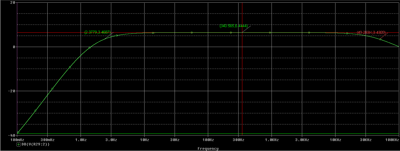
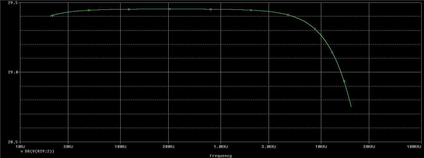
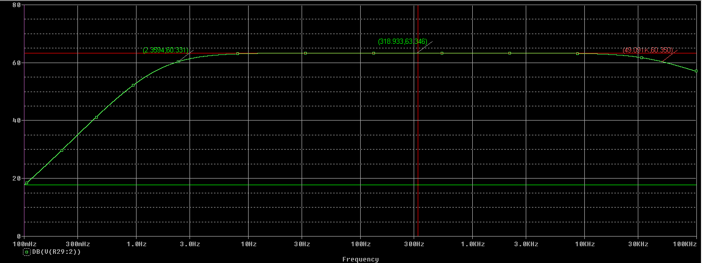
It is easy to measure the low frequency and high frequency -3dB points. EDIT: An audio amplifier is not measured up to 10GHz. I think this one is -3db at 80kHz that you cannot see on your very wide range of frequencies.
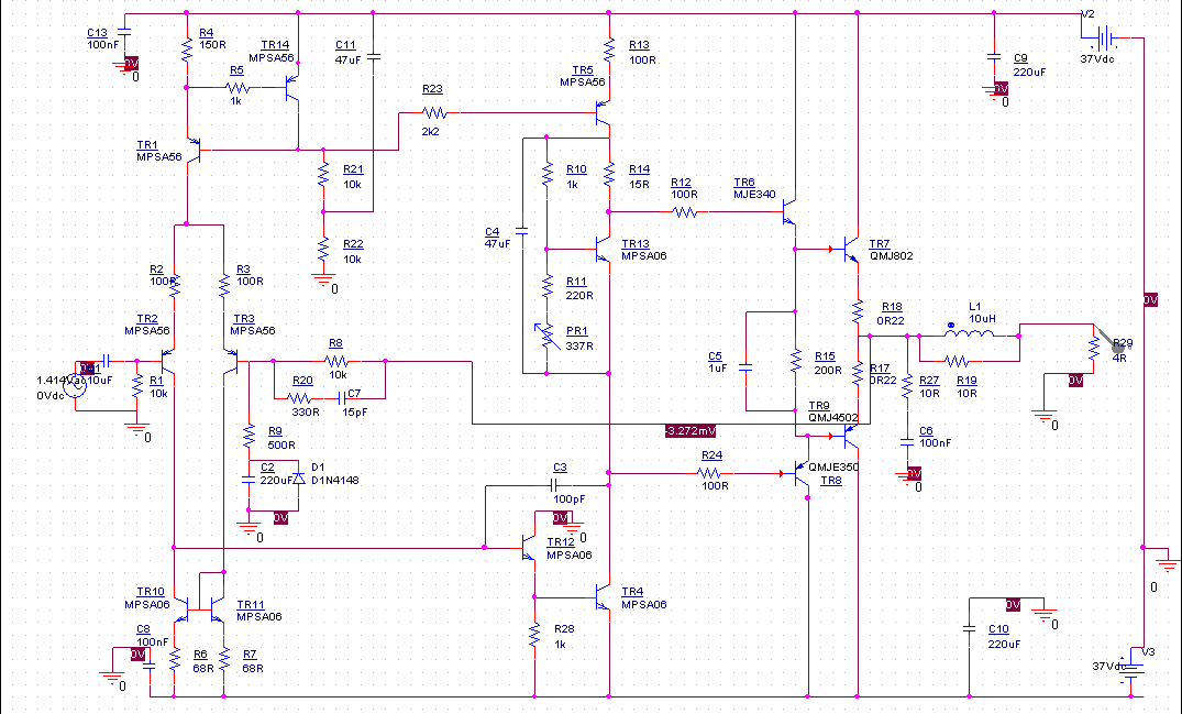
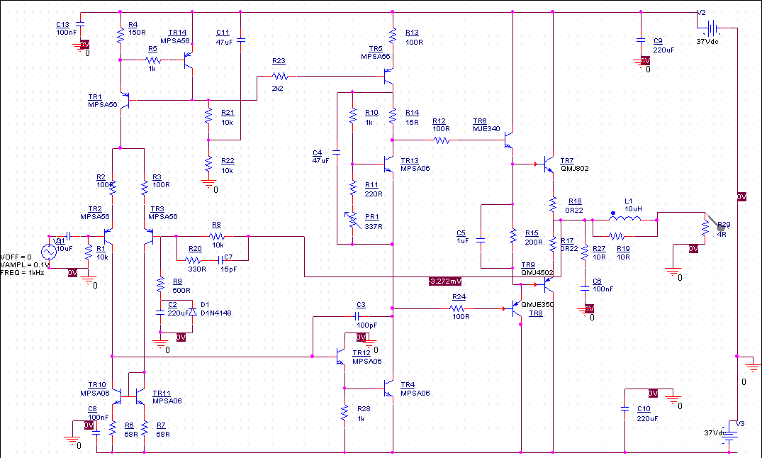
Maybe you should mention in your answer that this "blameless" amplifier was designed for 50W into 8 ohms and might be overloaded and might overheat with 110W into 4 ohms.
Thanks a lot for your speedy response, it's really appreciated! Thanks for the link to the article it was very useful and I had searched it before, however I hadn't realised that the component values were different from the ones he was referencing - hence I didn't immediately find the reference!
I'll be sure to mention the danger of overheating - it is a very crucial detail!
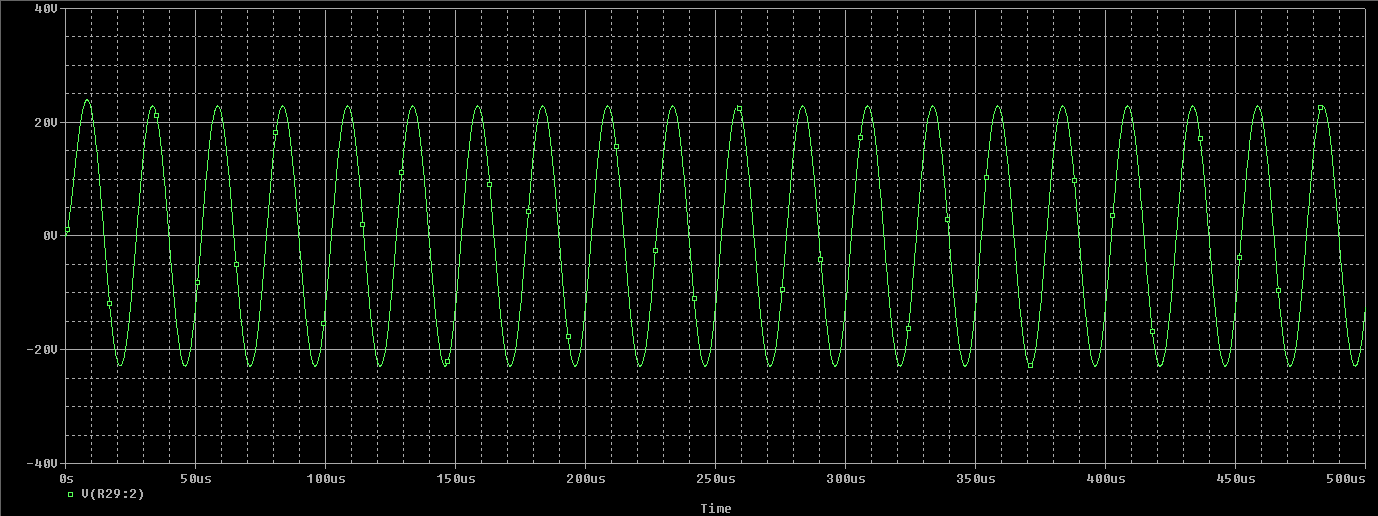
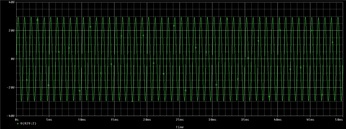
I had another go at measuring the bandwidth and came up with the attached images and corresponding traces. I calculated the bandwidth by finding the middle frequency and then the difference between the lower and upper bounds, despite changing the voltage from 0.1V to 1.414V the bandwidth changed very little, is this to be expected?
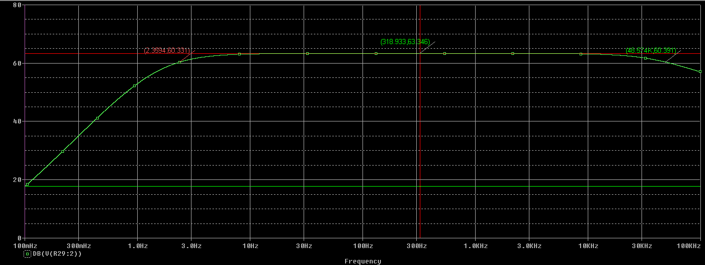
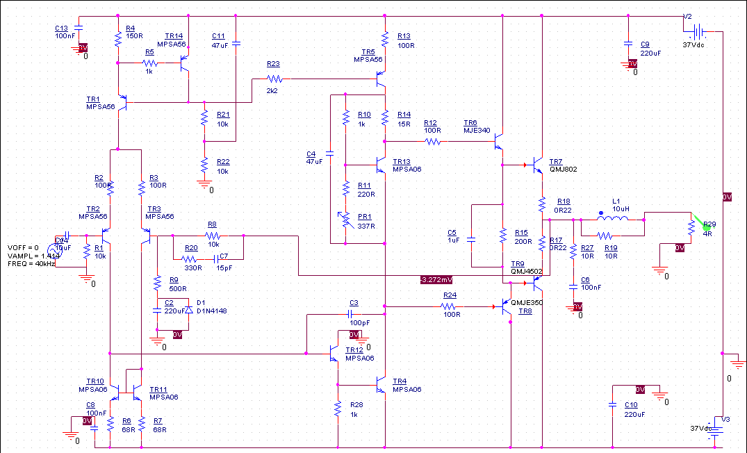
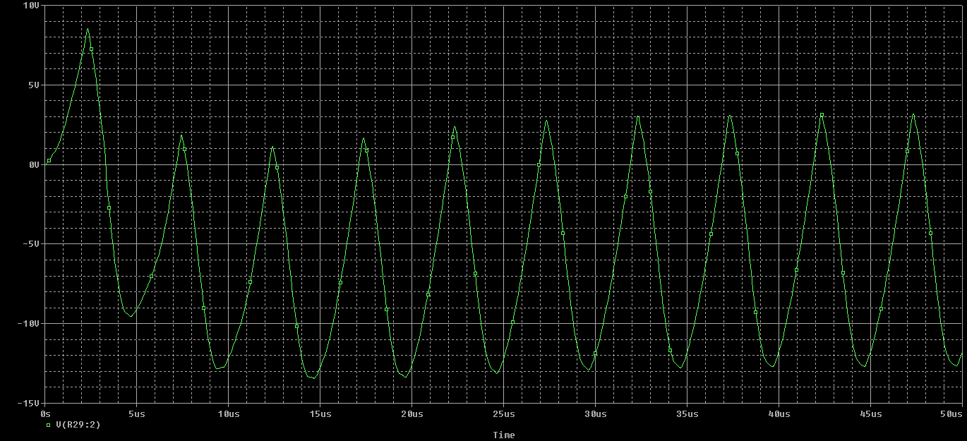
") I am not quite sure what you mean about there being no AC input to the simulation circuit. On the far left hand side there is an AC input of 0.1 V on the first example and 1.414V in the second example...
I am not quite sure what you mean about there being no AC input to the simulation circuit. On the far left hand side there is an AC input of 0.1 V on the first example and 1.414V in the second example...