sandeep pagare
Newbie level 4
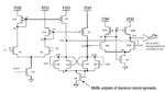
i have send comparator diagram with code and output. plz give me the output. biasing ckt (vbiasn) is given in the fig.20.15 in cmos layout book (jekob bekar). plz give me the output. the output show error. plz help me
****comparator*******
.options nomod node list brief POST ingold=1
.option scale=1u
.global control
.param pvdd=5
*****Power Supply********
VDD VDD 0 DC 5
Vp vp 0 DC 2.5 PULSE 2.46 2.54 125n 0 0 10n
vm vm 0 DC 2.5
vss vss 0 dc -5v
M1 n1 vp vss 0 NMOS L=1 W=10
M2 n2 vm vss 0 NMOS L=1 W=10
Ma vss vbiasn 0 0 NMOS L=2 W=20
M31 n1 n1 vdd vdd PMOS L=1 W=20
M41 n2 n2 vdd vdd PMOS L=1 W=20
M3 vop n1 vdd vdd PMOS L=1 W=20
M4 vom n2 vdd vdd PMOS L=1 W=20
M5 vop vop vc 0 NMOS L=1 W=10
M6 vop vom vc 0 NMOS L=1 W=10
M7 vom vop vc 0 NMOS L=1 W=10
M8 vom vom vc 0 NMOS L=1 W=10
Mb vc vc 0 0 NMOS L=10 W=10
M9L n4 vom n3 0 NMOS L=1 W=10
M9R vdo vop n3 0 NMOS L=1 W=10
M10L n4 n4 vdd vdd PMOS L=1 W=20
M10R vdo n4 vdd vdd PMOS L=1 W=20
Mc n3 n4 0 0 NMOS L=1 W=10
MIN out vdo 0 0 NMOS L=1 W=10
MIP out vdo vdd vdd PMOS L=1 W=20
.subckt bias vbiasn vbiasp VDD
M1 Vbiasn Vbiasn 0 0 NMOS L=2 W=10
M2 Vbiasp Vbiasn Vr 0 NMOS L=2 W=40
M3 Vbiasn Vbiasp VDD VDD PMOS L=2 W=30
M4 Vbiasp Vbiasp VDD VDD PMOS L=2 W=30
Rbias Vr 0 6.5k
MSU1 Vsur Vbiasn 0 0 NMOS L=2 W=10
MSU2 Vsur Vsur VDD VDD PMOS L=100 W=10
MSU3 Vbiasp Vsur Vbiasn 0 NMOS L=1 W=10
******TRANSIENT*******
.tran 100p 150n
.meas max_power max power
.measure TRAN risetime TRIG v(out) VAL='0.1*pvdd' rise=1 TARG V(out) VAL='0.9*pvdd' rise=1
.measure TRAN falltime TRIG v(out) VAL='0.9*pvdd' fall=1 TARG V(out) VAL='0.1*pvdd' fall=1
.lib 'E:\Spice_example\tsmccl013g_logic.spice' TT
.end
.include .\1um_models.txt
.end