giorgi3092
Junior Member level 2
Hi, I am cross posting this from Reddit because I did not get a full answer there.
I am starting to design a multistage differential LNA in a CMOS process. The textbooks (e.g. by Voinigescu) suggest that the first stage must always have lowest NF based on Frii's equation of cascades amplifier blocks. I get that.
He suggests that the way to start is to select the current density (mA/um) such that the noise figure is the minimum and if that current density is kept at that value, noise figure will remain constant (even irrespective of frequency in case of CMOS). He goes ahead and states that for CMOS processes, the value is almost constant and is about 0.15 mA/um (down to 65nm). Mine is 22nm, and it is expected to be a little more - up to 0.3 mA/um.
The issue I have is - how do I generate those nice plots of NF versus current density in Cadense? I see these figures in almost all LNA papers, but nobody shows the test fixture of this simulation. I am referring to such plots:

My idea is to throw in one transistor on the schematic - hook up bias tees at the gate and drain with proper drain voltage which seems to be max of 0.9 volts in my case. I also connect two 50 ohm ports at the input and output. I fix total gate width to 10 um for example, and vary gate voltage from 0.2 to 0.7 volts.
Then, I do S-parameter simulation at my design frequency (with noise enabled), choosing gate voltage as the sweep variable from 0.2 to 0.7 volts.
This way, I get NF versus Vgs, instead of NF versus current density. How do I plot NF versus current density? Should I change my test fixture?
Also, since I want the drain current to be varied logarithmically, it seems the sweep variable must be the drain current instead of gate voltage, but if I vary the drain current with a current source how do I set an appropriate gate voltage?
Has anyone done this before and can enlighten me?
Thank you.
EDIT:
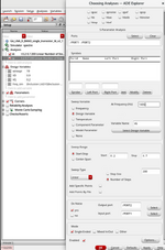
I will also supply my setup:

S-parameter simulation setup:

Does this look okay?
I am starting to design a multistage differential LNA in a CMOS process. The textbooks (e.g. by Voinigescu) suggest that the first stage must always have lowest NF based on Frii's equation of cascades amplifier blocks. I get that.
He suggests that the way to start is to select the current density (mA/um) such that the noise figure is the minimum and if that current density is kept at that value, noise figure will remain constant (even irrespective of frequency in case of CMOS). He goes ahead and states that for CMOS processes, the value is almost constant and is about 0.15 mA/um (down to 65nm). Mine is 22nm, and it is expected to be a little more - up to 0.3 mA/um.
The issue I have is - how do I generate those nice plots of NF versus current density in Cadense? I see these figures in almost all LNA papers, but nobody shows the test fixture of this simulation. I am referring to such plots:
My idea is to throw in one transistor on the schematic - hook up bias tees at the gate and drain with proper drain voltage which seems to be max of 0.9 volts in my case. I also connect two 50 ohm ports at the input and output. I fix total gate width to 10 um for example, and vary gate voltage from 0.2 to 0.7 volts.
Then, I do S-parameter simulation at my design frequency (with noise enabled), choosing gate voltage as the sweep variable from 0.2 to 0.7 volts.
This way, I get NF versus Vgs, instead of NF versus current density. How do I plot NF versus current density? Should I change my test fixture?
Also, since I want the drain current to be varied logarithmically, it seems the sweep variable must be the drain current instead of gate voltage, but if I vary the drain current with a current source how do I set an appropriate gate voltage?
Has anyone done this before and can enlighten me?
Thank you.
EDIT:
I will also supply my setup:
S-parameter simulation setup:
Does this look okay?
Attachments
Last edited: