Welcome to our site! EDAboard.com is an international Electronics Discussion Forum focused on EDA software, circuits, schematics, books, theory, papers, asic, pld, 8051, DSP, Network, RF, Analog Design, PCB, Service Manuals... and a whole lot more! To participate you need to register. Registration is free. Click here to register now.
Hi every body,
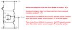
This is a opamp output voltage booster schematic but I can not understand how each part work ,if any one can analysis this circuit please explain it for me in detail.
It is a very simple audio power amplifier circuit with a differential input. You need to learn about the basics of transistors to understand how each part works.
It contains sections which are typical in an op amp. As Audioguru states, it has the differential input (long-tail pair).
The rightmost two transistors are a half-bridge. This resembles the final output stage of an op amp. The correct biasing comes from the section in the center (diodes, resistors, transistor).
An amplifier is usually destroyed if it is playing and the output is shorted because then the output current will become much too high. Diodes D3 and D4 were added to limit the maximum output current like this:
This site uses cookies to help personalise content, tailor your experience and to keep you logged in if you register.
By continuing to use this site, you are consenting to our use of cookies.