Welcome to our site! EDAboard.com is an international Electronics Discussion Forum focused on EDA software, circuits, schematics, books, theory, papers, asic, pld, 8051, DSP, Network, RF, Analog Design, PCB, Service Manuals... and a whole lot more! To participate you need to register. Registration is free. Click here to register now.
Re: Please explain difference between these two 2stag op-amp
Hi yonzzan,
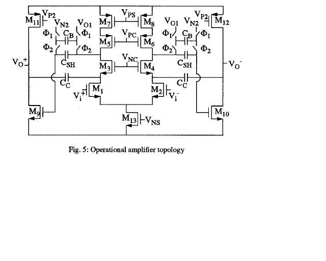
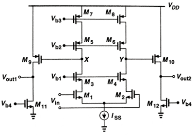
A switched-capacitor level-shifter is utilized in first cicuit in order to use nMOS transistor as the input devices of both stages (Since there are two pMOS trs. and three nMOS trs. stacked in the first stage, the output CM voltage of the first stage is usually much larger than Vtn (threshold voltage of nMOS device) but low enough for driving a pMOS as in the second diagram. However, if a folded-cascode structure is used as the first stage, this problem won't occur). This is due to the usual higher mobility => higher gm => higher speed of nMOS devices compared to their pMOS counterparts. However, in new low-voltage applications, let's say less than 1.2 V, no level shifter is required since the output voltage of the first stage would be suitable for an nMOS input device of the second stage. On the other hand, this special level shifter limits the use of this circuit to sampled-data applications, where the opamp works in one phase and resets in the other (switched cap. structures usually produce glitches if applied to continuous-time applications which is not tolerable in many applications).
BTW, it seems something is missing in the second circuit. No compensation cap. exists in this diagram! (maybe it is not sketched for simplification)
This site uses cookies to help personalise content, tailor your experience and to keep you logged in if you register.
By continuing to use this site, you are consenting to our use of cookies.