biff44
Advanced Member level 6
- Joined
- Dec 24, 2004
- Messages
- 5,047
- Helped
- 1,376
- Reputation
- 2,748
- Reaction score
- 1,056
- Trophy points
- 1,393
- Location
- New England, USA
- Activity points
- 37,909
Hi,
I don't know what you want me to explain.
A capacitor, a scope probe, a TIA, why a TIA improves fall time?
Everything already is explained. Do a forum search, do an internet search first.
If then still are questions you are welcome to ask a detailed question. Please refer to documents you have read, so we can discuss about it.
Klaus
Op-Amp Transimpedance Amplifier
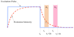
A transimpedance amplifier (TIA) converts a current to a voltage and is often used with current-based sensors like photodiodes. It’s also a common building block that helps explain the performance and stability limits of many other op-amp circuits.
the input impedance of a transimpedance amplifier is NOT zero at high frequencies. so, where exactly do you expect that stored charge in the photodetector to go? to Disney world?