sk.shawn
Junior Member level 3
Hi erikl & FvM,
Thank you so much for the responses. However, I still have some doubts on the operating aspect of this circuit. In addition, I will explain my take on the overall design of my circuit.
Thanks for pointing out that. As a matter of fact, I do not have the option to work with dual supplies. And so, I'm dealing with only a single supply (0V-3.3V) to realize everything.
Now, what you've said makes perfect sense and I fully agree with it. In fact, I have tried this way too in one of my many iterations earlier. But, it seems like the opamp output will stay saturated at 3.3V when:
Vp = Vin = 1V
I chose this value instead of (VDD-GND)/2 as it was the common mode value designed and tested for in my earlier opamp simulation (as attached here). Hope this is ok?
Now with that above done, I also grounded the Vref input to the FCC. The entire test setup for this simulation run is shown below
It's basically the same setup as before and I did not include any feedback resistor as I wanted to stay consistent to the original paper's design. Unless, for my case, the feedback resistor is needed due to my common input voltage range?
Back to the same doubt, by having such a setup, how will it allow me to vary Vin and obtain a range of voltage values from 1.2V to 2.2V at the opamp output?
I mean all this while, I've been visualizing this circuit's operation as:
Vin is a range of small DC voltage values that will correspond to an opamp output of 1.2V to 2.2V so that the VCO can be drived. Of course, I will have to adjust and calibrate until I find the range of values for Vin corresponding to the intended opamp output range (1.2V - 2.2V)
Is my visualization correct? Please advise me further. Thanks
Thanks for the support and advise given FvM. Unfortunately, for my circuit, I have to work with a single supply (0V - 3.3V). So, as mentioned above I fed Vin and Vp both a 1V DC voltage and grounded Vref. With that, the opamp output went saturated at 3.3V.
I was thinking maybe my understanding of the circuit, as in the manner in which Vin comes in and influence the opamp output is incorrect (as described above)?
Also, I would like to hear from you if my FCC is functioning correctly based on the measurements and the circuit I've designed?
Guys, thanks a lot for coming into my thread and helping out consistently. I feel that at least there is some form of progression. I just hope eventually this circuit can work out since the author has demonstrated the functionality of this topology in his paper. I look forward to all of your replies.
Appreciate it!
Regards,
Shawn
Thank you so much for the responses. However, I still have some doubts on the operating aspect of this circuit. In addition, I will explain my take on the overall design of my circuit.
erikl said:your opAmp - contrary to that one used in the original paper (LM324) - does not include GND in its common input voltage range. I think its min. common input voltage is about Vth(nmos)+Vds(M13a). So if you'd tie Vin as well as Vp to a voltage greater than this min. common input voltage - say (VDD-GND)/2 , and the Vref input of your (now: ) FCC to a lower voltage (may be GND), perhaps this could achieve the required negative feedback mentioned by FvM.
Not sure about this; perhaps FvM can comment?
erikl
Thanks for pointing out that. As a matter of fact, I do not have the option to work with dual supplies. And so, I'm dealing with only a single supply (0V-3.3V) to realize everything.
Now, what you've said makes perfect sense and I fully agree with it. In fact, I have tried this way too in one of my many iterations earlier. But, it seems like the opamp output will stay saturated at 3.3V when:
Vp = Vin = 1V
I chose this value instead of (VDD-GND)/2 as it was the common mode value designed and tested for in my earlier opamp simulation (as attached here). Hope this is ok?
Now with that above done, I also grounded the Vref input to the FCC. The entire test setup for this simulation run is shown below
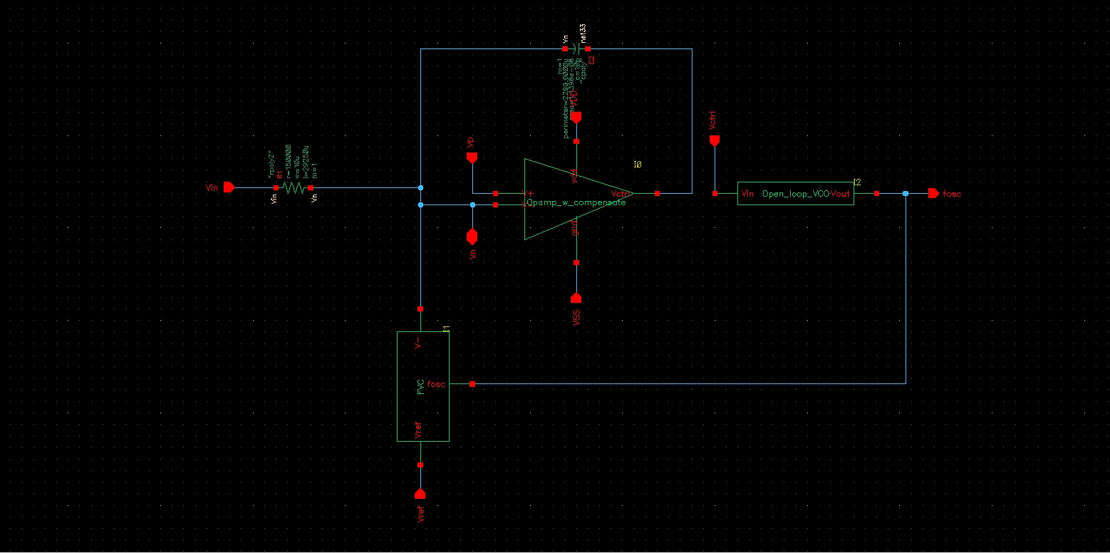
It's basically the same setup as before and I did not include any feedback resistor as I wanted to stay consistent to the original paper's design. Unless, for my case, the feedback resistor is needed due to my common input voltage range?
Back to the same doubt, by having such a setup, how will it allow me to vary Vin and obtain a range of voltage values from 1.2V to 2.2V at the opamp output?
I mean all this while, I've been visualizing this circuit's operation as:
Vin is a range of small DC voltage values that will correspond to an opamp output of 1.2V to 2.2V so that the VCO can be drived. Of course, I will have to adjust and calibrate until I find the range of values for Vin corresponding to the intended opamp output range (1.2V - 2.2V)
Is my visualization correct? Please advise me further. Thanks
FvM said:Yes, Vref-Vp is the effective reference voltage driving the frequency-to-current converter. And of course a positive Vp related
to Vs would be needed with the NMOS differential input stage. Vp would be also the reference for Vin. I think, the best solution
depends on the overall design. With a dual supply, as stated above, the circuit can work with Vp=0 as well, but then requires a
negative Vref.
Thanks for the support and advise given FvM. Unfortunately, for my circuit, I have to work with a single supply (0V - 3.3V). So, as mentioned above I fed Vin and Vp both a 1V DC voltage and grounded Vref. With that, the opamp output went saturated at 3.3V.
I was thinking maybe my understanding of the circuit, as in the manner in which Vin comes in and influence the opamp output is incorrect (as described above)?
Also, I would like to hear from you if my FCC is functioning correctly based on the measurements and the circuit I've designed?
Guys, thanks a lot for coming into my thread and helping out consistently. I feel that at least there is some form of progression. I just hope eventually this circuit can work out since the author has demonstrated the functionality of this topology in his paper. I look forward to all of your replies.
Appreciate it!
Regards,
Shawn