Continue to Site

Welcome to EDAboard.com

Welcome to our site! EDAboard.com is an international Electronics Discussion Forum focused on EDA software, circuits, schematics, books, theory, papers, asic, pld, 8051, DSP, Network, RF, Analog Design, PCB, Service Manuals... and a whole lot more! To participate you need to register. Registration is free. Click here to register now.

Need help with my circuit

Status
Not open for further replies.

sk.shawn

Junior Member level 3
Joined
May 4, 2008
Messages
30
Helped
1
Reputation
2
Reaction score
1
Trophy points
1,288
Activity points
1,689
Dear all,


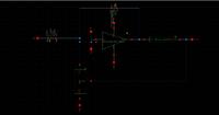
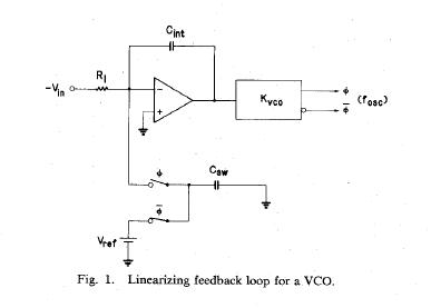
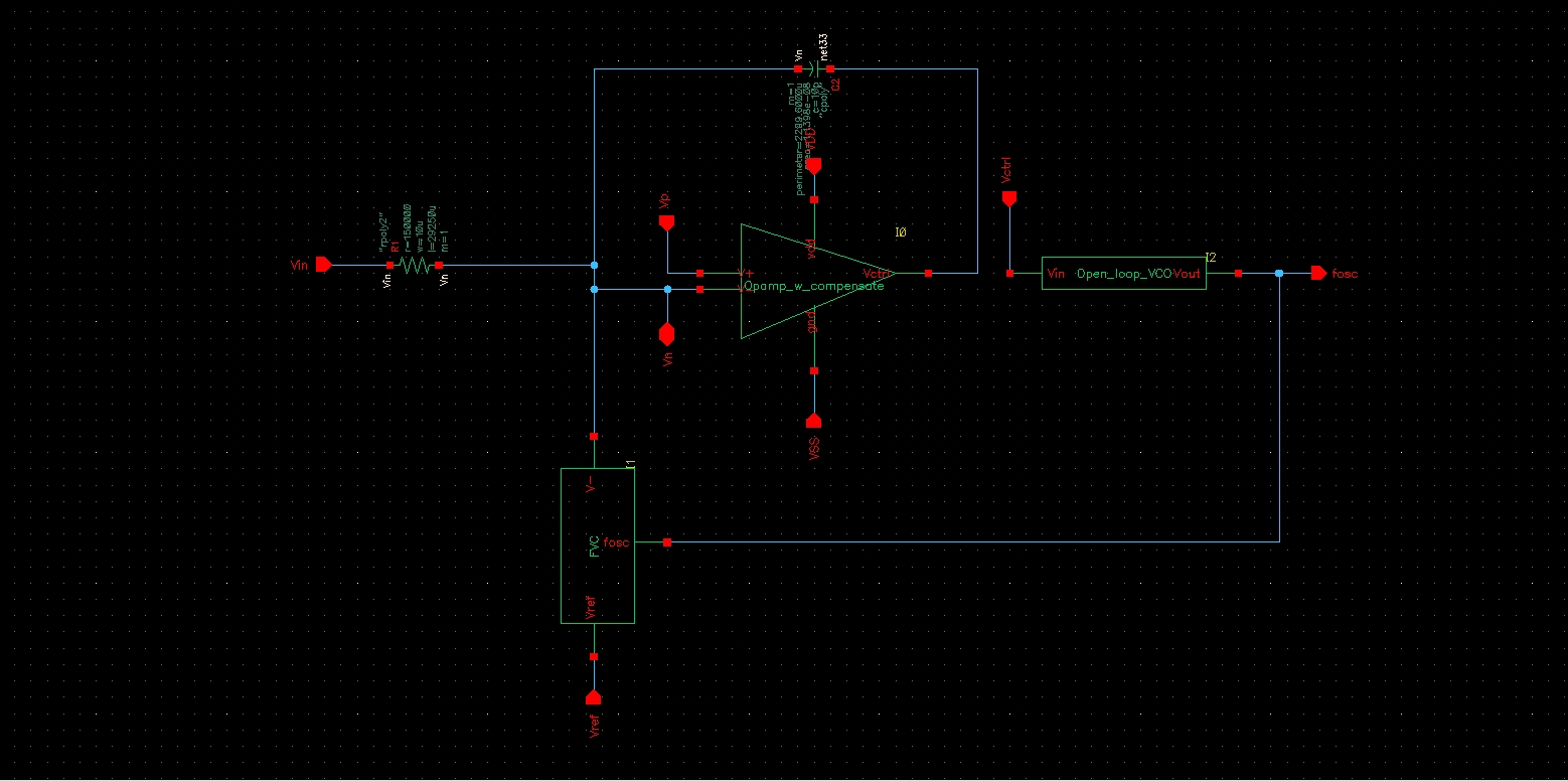
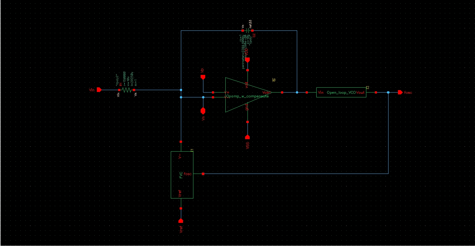
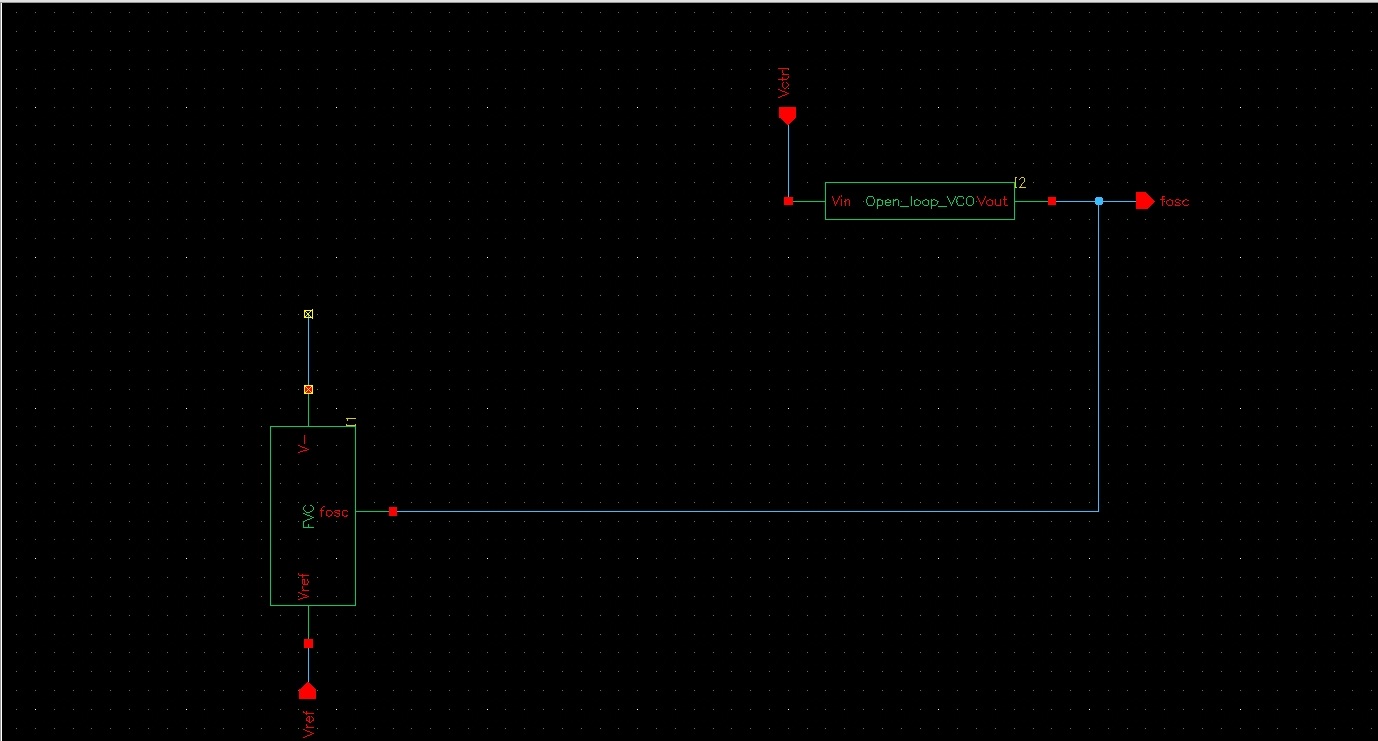
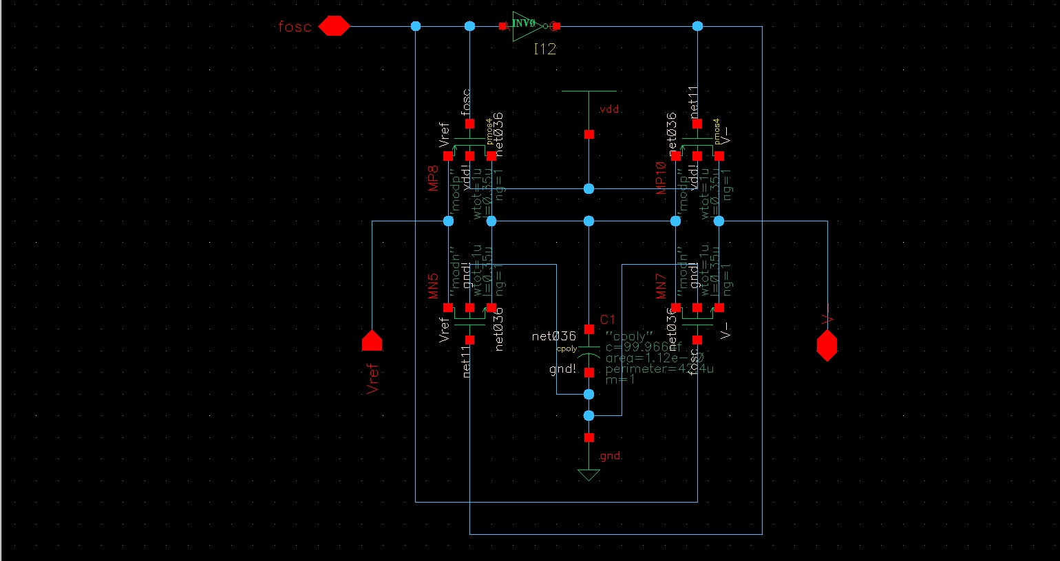
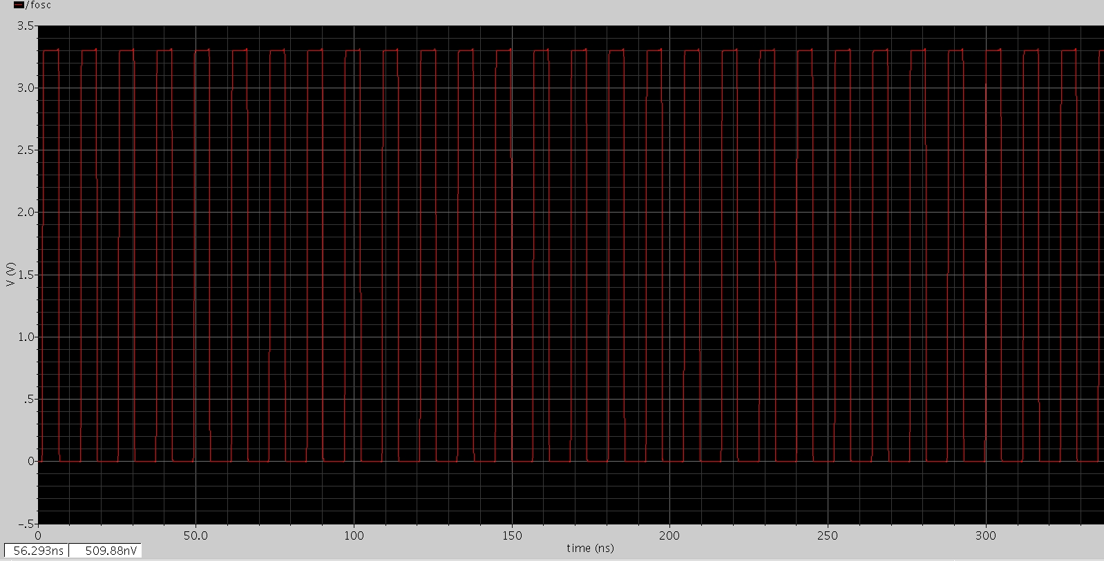
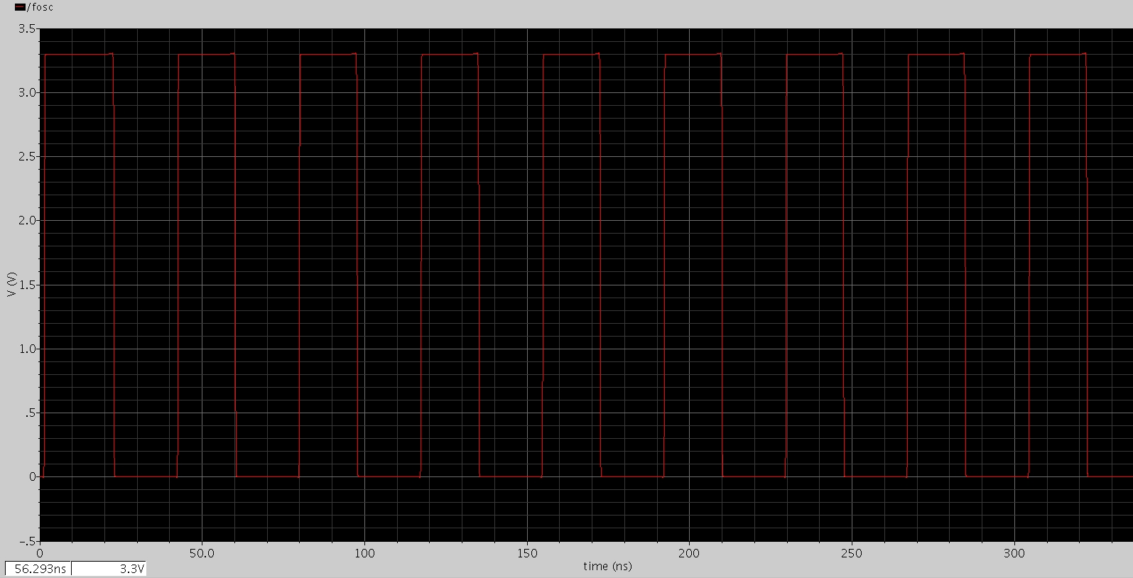
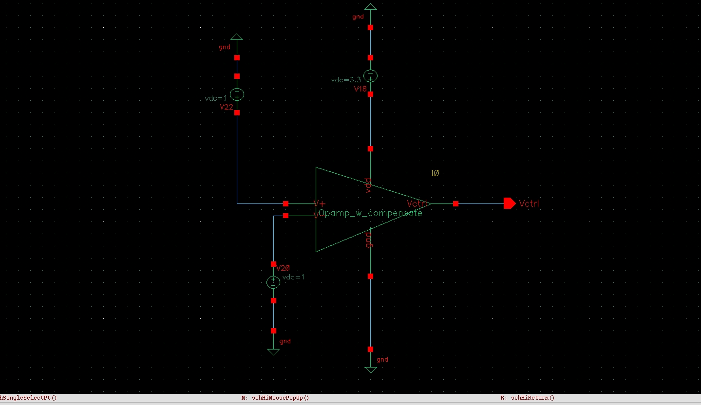
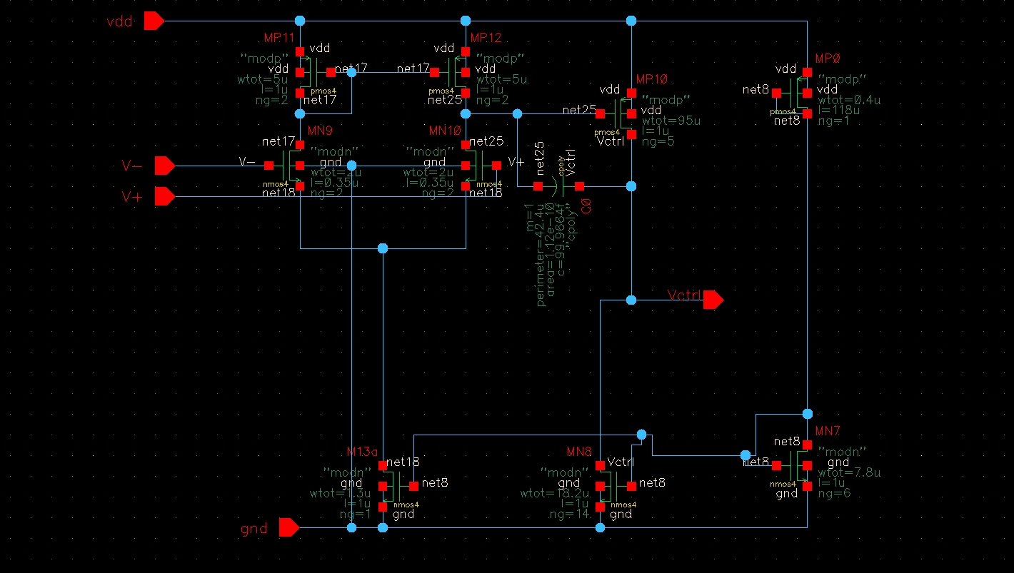
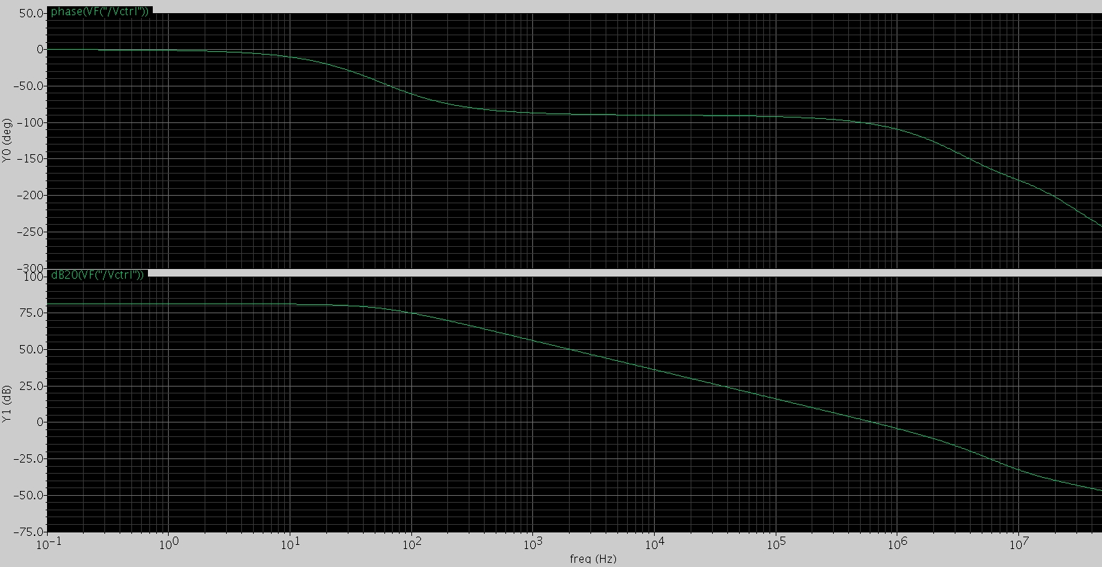
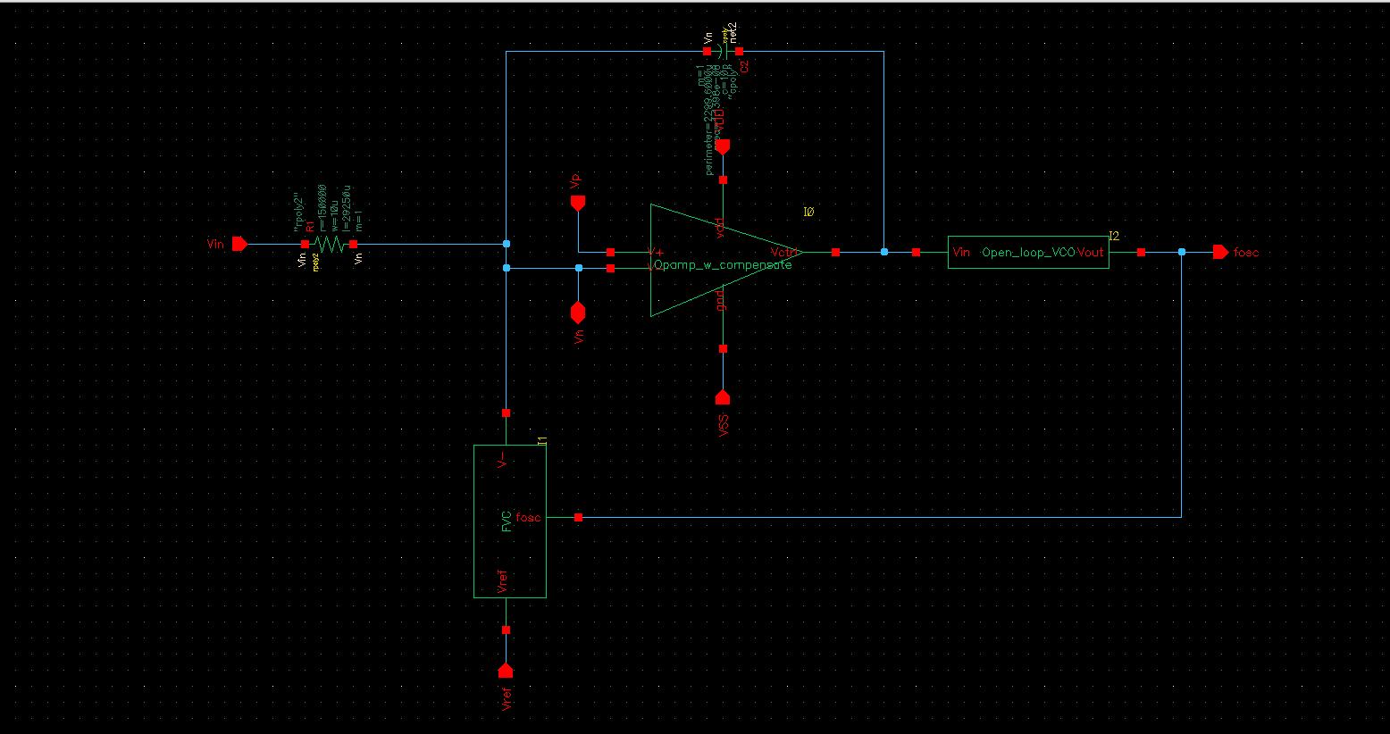
I'm seriously having problems with this circuit (as attached) that I'm designing at the moment. The topology is based on a paper reported in solid state journal and the working principle is to linearize my open loop VCO by negative feedback using a switched capacitor network that is acting as a frequency to voltage converter (FVC).

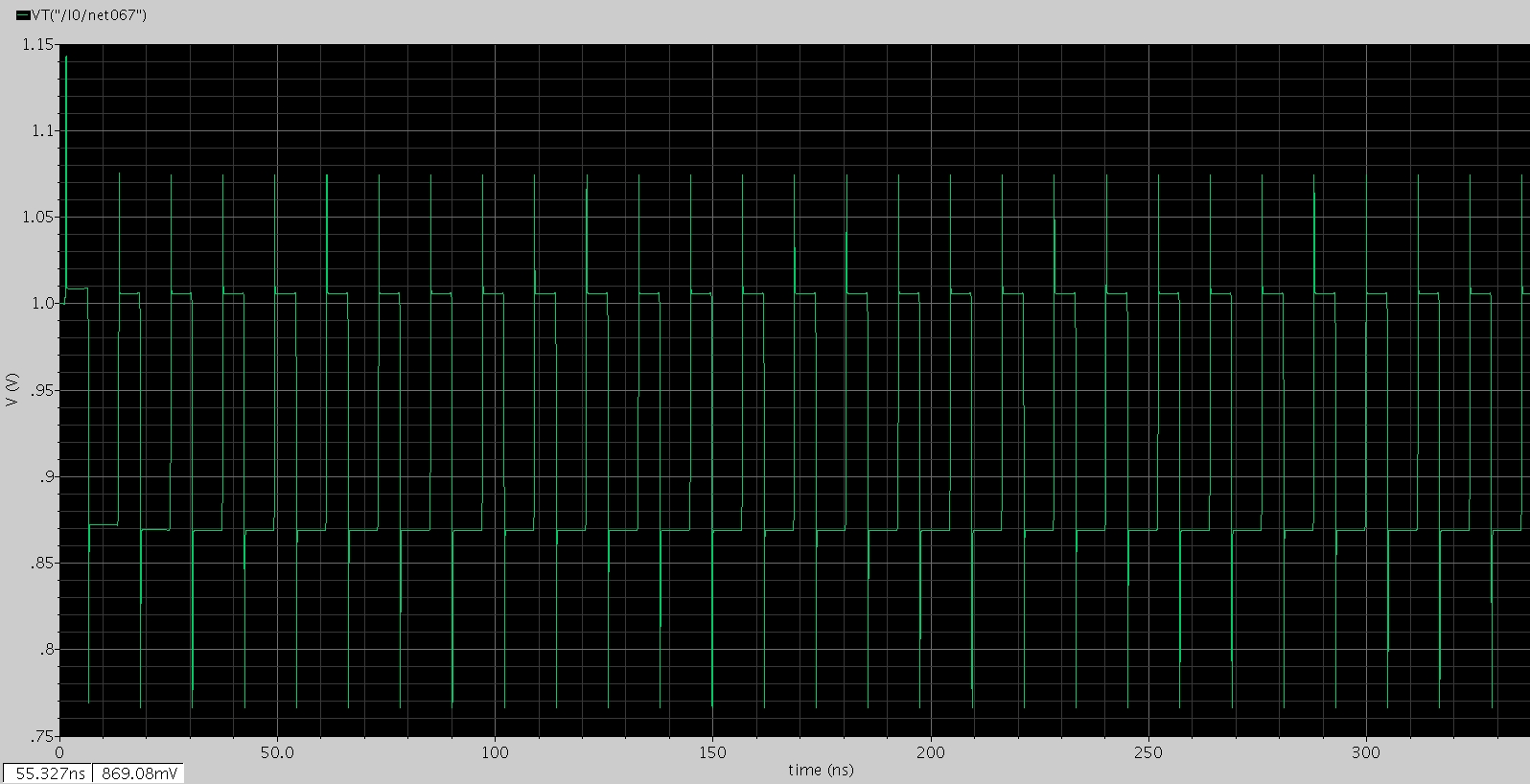
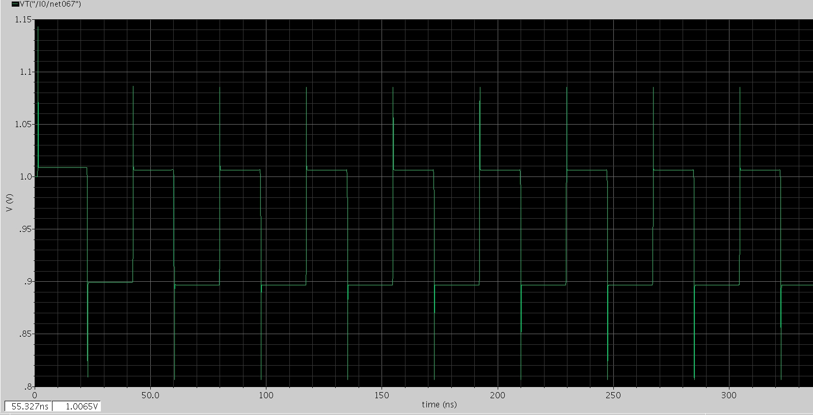
The issue is can Vin be a DC signal? As soon as I feed a DC input, the opamp output is immediately saturated. I'm just all confused about the type of input signal that should be fed. Ultimately, the range of voltage that I would like to have at the opamp output is 1.2V to 2.2V which I have no idea of how to achieve this.

I have tested all individual blocks separately and they are all working (opamp, FVC, open loop VCO). I feel that it could be just some minor thing that I need to get it figured out. So, I'm hoping someone here can shine some light to assist me.

P.S Vin is a negative input.

Sorry for the long type. Any help is appreciated greatly.

Thanks a million.

Regards,
Shawn
 

sk.shawn said:
Dear all,
...I have tested all individual blocks separately and they are all working (opamp, FVC, open loop VCO). I feel that it could be just some minor thing that I need to get it figured out... Shawn
Sorry, but I must ask you:
do you have pls at your OpAmp resistors too?
K.
 

    sk.shawn

    Points: 2
    Helpful Answer Positive Rating
karesz said:
do you have pls at your OpAmp resistors too?

Hi,

Thanks for replying. I'm sorry but I didnt really get your question.

What is meant by "pls at your opamp resistors"? I'm rather new so I may not be familiar with some terminologies.

Appreciate your revert and support.

Regards,
Shawn
 

Dear all,

48_1262605718.jpg


I reckon it would be clearer to attach the exact same schematic taken from the paper that I had referenced on. It's shown above.

Considering this circuit, what kind of response should I expect at the opamp output? Is it possible to generate a range of values say from 1.2V-2.2V at the opamp output? If so, what should the input signal Vin be?

From the loop dynamics dervied,

(Vin/R - fosc*Csw*Vref) * 1/sCint = Vctrl

So I was thinking, to obtain my desired range of 1.2V to 2.2V at the opamp output, I can fix Vctrl to any of the values in the range and solve for Vin. To me, Vin should be an ac signal with a well-defined frequency due to the 's' parameter in the loop equation above. So, I tried feeding it with a sine wave of say 1kHz with the appropriate amplitude Vin corresponding to the required Vctrl value I want. But it doesnt work in that way. So I'm like confused now. :(

For the record, I've chosen R1 as 150K, Cint as 10pF and Csw as 0.1pF. The capacitor switched network has been tested independently and it's ok.

Can some kind experts help me out with the analysis of this circuit and guide me accordingly. Really appreciate it. I'll be more than willing to provide further information if required.

And sorry for the repeated post as I've really exhausted my means. I've been stuck on this for the past 2 weeks.

Any help is welcomed. Thanks a lot.

Regards,
Shawn
 

sk.shawn said:
... Ultimately, the range of voltage that I would like to have at the opamp output is 1.2V to 2.2V
You are operating your opamp in open loop integrating configuration, which means it might have a DC gain of 80 or even 100dB, i.e. an input change in the order of only -10µV .. -100µV can cause your required output change from 1.2 to 2.2V.

In order to find the correct operating point (by adjusting Vp @ V+), you should first decrease the DC gain of your opamp by using a feedback resistor in parallel to the integration capacitor C2. (I guess this is the reason for karesz' question above.) The value of this resistor depends on the output resistance at the V- output of your FVC, but a value in the order of 100kΩ .. 1MΩ should be fine for the beginning.

Then adjust Vp (@ the V+ input of the opamp) by means of a voltage divider (potentiometer) so that your opamp output voltage achieves the required low value (1.2V) when the FVC receives the appropriate corner frequency.

Then switch your VCO (open loop) to the other corner frequency which should correspond to an opamp output voltage of 2.2V. Adjust the required 2.2V output voltage by adjusting the a.m. feedback resistor value to an appropriate value.
 

    sk.shawn

    Points: 2
    Helpful Answer Positive Rating
Hi erikl,

Many thanks for your reply. However, there are still some points that I'm quite unclear about. Hope you will continue to guide me along.

As a matter of fact, I did try to include the feedback resistor earlier before my post. However, from the paper alone, the author has not included any feedback resistor. So, I felt the move to include the feedback resistor may not be right and thus I threw out that idea

Now after you have explained it, it seems to me that this circuit may require a feedback resistor. However, there is another issue now if I had interpreted your explanation correctly and that is there is a need to repeatedly calibrate the feedback resistor along with Vp to achieve the required range of values at the opamp output.

In that case, how will the input voltage Vin fit in? Besides, Vp according to the paper is grounded. In fact, I was thinking of fixing all other parameters in the circuit with just only Vin varying to achieve the required range of values at the opamp output. Is my way of thinking wrong? Please advise me. Thanks!

P.S I've uploaded the paper for your reference too. Hope it will be of help.

Appreciate again for the reply.

Regards,
Shawn
 

In my opinion, saturation of integrator output (you don't observe oscillations, as far as I understand) means, that the F/I
feedback either doesn't work at all, has wrong polarity, or doesn't source enough current to compensate the input signal.
You may want to check the feedback circuit in open loop first.
 

    sk.shawn

    Points: 2
    Helpful Answer Positive Rating
erikl said:
sk.shawn said:
... In order to find the correct operating point (by adjusting Vp @ V+), you should first decrease the DC gain of your opamp by using a feedback resistor in parallel to the integration capacitor C2. (I guess this is the reason for karesz' question above.) The value of this resistor depends on the output resistance at the V- output of your FVC, but a value in the order of 100kΩ .. 1MΩ should be fine for the beginning.
Yes & Thnx Erikl!
You know-my english is some time more to deshifring _worser as possible...:-( Sorry!
K.
 

    sk.shawn

    Points: 2
    Helpful Answer Positive Rating
Hi shawn,

with your schematic and the paper it's much clearer now, thank you! Seeing now that your FVC together with the opamp is a proper switched-capacitor circuit, you probably don't need a feedback resistor. And as it's not a full chip design (as I reckoned before, because most of the threads in this forum are), you have no problem to inject a (small) negative DC voltage at the Vin input, hence no operating point adjustment at the Vp=V+ input is necessary. So I suggest the following procedure to adjust the operating point resp. range:

During the adjustment, keep the VCO in open loop, i.e. break the loop between the opAmp output and the VCO input. Control the VCO for the desired frequencies by inserting an appropriate DC input voltage.

1. Put the VCO to the lower corner frequency. Measure the necessary DC control voltage - let's say it's 1.2V .

2. Then - at the Vin input - without applying a sinus ac voltage - adjust a (probably small) negative DC voltage which generates the required opamp output voltage of 1.2V . This calibration procedure has to be done only once or just for a few iterations (s. below). Then this voltage should be fix forever.

3. Now push the VCO output by an appropriate DC control voltage at its Vin input to the desired upper corner frequency. Let's say the necessary control voltage now is 2.2V.

4. Now measure the opamp output voltage at this upper corner frequency. If it's also close to 2.2V, you're already done. If it's too for away, you can adjust it by changing the Csw/Cint ratio, which defines the ac gain of the opamp. If your opamp output is too high, reduce Csw, if too low, increase it.

5. If you had to adjust Csw, you possibly must readjust the -Vin voltage, i.e. iterate from point 1 to 4 above.

When your operating range adjustment is ok, you can close the loop and it should work. Applying an additional (capacitively coupled!) ac voltage at the -Vin input shouldn't change the operating point.

Hope this helps. Good luck! erikl
 

    sk.shawn

    Points: 2
    Helpful Answer Positive Rating
erikl said:
Hi shawn,

with your schematic and the paper it's much clearer now, thank you! Seeing now that your FVC together with the opamp is a proper switched-capacitor circuit, you probably don't need a feedback resistor. And as it's not a full chip design (as I reckoned before, because most of the threads in this forum are), you have no problem to inject a (small) negative DC voltage at the Vin input, hence no operating point adjustment at the Vp=V+ input is necessary. So I suggest the following procedure to adjust the operating point resp. range:

During the adjustment, keep the VCO in open loop, i.e. break the loop between the opAmp output and the VCO input. Control the VCO for the desired frequencies by inserting an appropriate DC input voltage.

1. Put the VCO to the lower corner frequency. Measure the necessary DC control voltage - let's say it's 1.2V .

2. Then - at the Vin input - without applying a sinus ac voltage - adjust a (probably small) negative DC voltage which generates the required opamp output voltage of 1.2V . This calibration procedure has to be done only once or just for a few iterations (s. below). Then this voltage should be fix forever.

3. Now push the VCO output by an appropriate DC control voltage at its Vin input to the desired upper corner frequency. Let's say the necessary control voltage now is 2.2V.

4. Now measure the opamp output voltage at this upper corner frequency. If it's also close to 2.2V, you're already done. If it's too for away, you can adjust it by changing the Csw/Cint ratio, which defines the ac gain of the opamp. If your opamp output is too high, reduce Csw, if too low, increase it.

5. If you had to adjust Csw, you possibly must readjust the -Vin voltage, i.e. iterate from point 1 to 4 above.

When your operating range adjustment is ok, you can close the loop and it should work. Applying an additional (capacitively coupled!) ac voltage at the -Vin input shouldn't change the operating point.

Hope this helps. Good luck! erikl

Hi erikl,

Thank you so much for the effort in drafting the step by step procedure to assist me. Sorry for the late update as I went on today enthusiastically to test things out as soon as I saw your revert. Now, I do hope I got my understanding right based on your explanation while I was carrying out my simulation for the whole of today. But still, just to be safe, I would like to re-iterate whatever I have done today and if I do get any steps wrong, please do not hesitate to correct me.

Attached right below is the circuit that was mentioned earlier where the VCO is kept in open loop (i.e. break the loop between the opAmp output and the VCO input)


I hope I got this point right?

Assuming it to be, I proceeded on by feeding Vctrl (i.e. the explicit input now to the VCO) the lower value of my intended range (i.e. 1.2V). This in turn generates an oscillating signal whose frequency is about 90MHz. Now the next step, if I didn't misunderstand your explanation is to start adjusting Vin which is a small negative DC voltage in this case. I did the adjustment until I saw a 1.2V appearing at the opamp output and the Vin value found is 9.8uV.

And next, I did the exact same thing for the upper value of my intended range (i.e 2.2V). Again, I fed 2.2 to Vctrl which generated an oscillating signal whose frequency is about 77MHz. After which, I did the same thing of adjusting Vin again until I saw a 2.2V appearing at the opamp output and this Vin value now is 341uV.

So, in sum, we have

Vin = 9.8uV (lower) -> 1.2V @ opamp output
Vin = 341uV (upper)-> 2.2V @ opamp output

I have a feeling that I may have got it wrong at this stage already. Please let me know if I did.

Assuming it again to be correct thus far, at this point, it's time to connect back the loop which is shown in the image below


So the loop is reconnected back now and I can start applying those Vin values (lower and upper) found earlier which will correspond to an opamp output voltage of 1.2V and 2.2V respectively. And as a matter of fact, the circuit is functioning in that way and there is oscillation. However, I just want to be sure that my understanding of your suggested approach is correct. Please comment at any stage of my message if I had done anything wrong. Thanks a million

P.S An important thing that I left out initially. For just testing now, I'm powering my opamp with dual supplies (i.e 2.5V and -2.5V) while the rest of the circuits (FVC and VCO) are operating in single supply with a value of 3.3V. In fact, the entire circuit should be just operating in 3.3V supply where I will eventually power the opamp also using a single 3.3V supply. But since, I'm at this stage of figuring out things, I just wanted to get the idea first. Will this supply thing be an issue? Just to let you know, the reason for powering the opamp using dual supplies initially is, to me, for simplicity sake since Vp is grounded. I reckon having dual supplies would be an easy way to get around the biasing of the input transistors of the opamp. Please let me know if there are any issues with this?

I'm really sorry for the terribly long post. I really appreciate the time devoted in assisting me. I really want to learn and hope I will master as much as I can from all of you.

Thanks once again. I look forward to your advise and support.

Regards,
Shawn
 

Seems like you don't want to verify the operation of the feedback circuit? I don't understand why.

If you finally succeed to operate the circuit, can you kindly report, if one of my guesses about it's failure have been correct.
 

    sk.shawn

    Points: 2
    Helpful Answer Positive Rating
Hi Shawn,
sorry, you didn't get me right. pls. s . below:

sk.shawn said:
Attached right below is the circuit that was mentioned earlier where the VCO is kept in open loop (i.e. break the loop between the opAmp output and the VCO input)


I hope I got this point right?
Yes, perfectly.

sk.shawn said:
Assuming it to be, I proceeded on by feeding Vctrl (i.e. the explicit input now to the VCO) the lower value of my intended range (i.e. 1.2V). This in turn generates an oscillating signal whose frequency is about 90MHz. Now the next step, if I didn't misunderstand your explanation is to start adjusting Vin which is a small negative DC voltage in this case. I did the adjustment until I saw a 1.2V appearing at the opamp output and the Vin value found is 9.8uV.
Still correct, as I suggested.
However, this voltage is very small, and probably much too sensible to be fixed forever (and that's what it should be!). In this case, I'd really suggest to use a feedback resistor (as I suggested before). I'd recommend to use a value Rfb which results in a dc gain of 10 .. 100, i.e. Rfb = 1.5 .. 15MΩ. This will shift the necessary -Vin (or +Vin, s. my last point below) input voltage from 9.8µV to a value in the order of 10 .. 100mV, which is much easier to be stabilized and kept. See my point 2. above: "Then this voltage should be fix forever."
Now the next point is where you misunderstood me:

sk.shawn said:
And next, I did the exact same thing for the upper value of my intended range (i.e 2.2V). Again, I fed 2.2 to Vctrl which generated an oscillating signal whose frequency is about 77MHz. After which, I did the same thing of adjusting Vin again until I saw a 2.2V appearing at the opamp output and this Vin value now is 341uV.
No! I didn't suggest to readjust -Vin ! The old value must be kept! Keeping the old -Vin value, you should just measure the new opAmp output voltage resulting from the new 77MHz frequency controlled by the open loop 2.2V input voltage to the VCO. Thoroughly re-read my point 4. above, and - if necessary - make the iteration steps as mentioned in point 5.
PS: Exchange "lower" and "upper" frequency corners in my instructions above - I couldn't know that there exists an inversion in your FVC.

sk.shawn said:
P.S An important thing that I left out initially. For just testing now, I'm powering my opamp with dual supplies (i.e 2.5V and -2.5V) while the rest of the circuits (FVC and VCO) are operating in single supply with a value of 3.3V. In fact, the entire circuit should be just operating in 3.3V supply where I will eventually power the opamp also using a single 3.3V supply. But since, I'm at this stage of figuring out things, I just wanted to get the idea first. Will this supply thing be an issue? Just to let you know, the reason for powering the opamp using dual supplies initially is, to me, for simplicity sake since Vp is grounded. I reckon having dual supplies would be an easy way to get around the biasing of the input transistors of the opamp. Please let me know if there are any issues with this?
Actually - in my first posting to your thread - I reckoned you'd design a full chip system which has to get along with one single power supply. This of course is also possible with your discreetly built system: Just provide the operating point calibration at the V+ input of your opAmp, as I adviced you in my first posting. In this case you may use a single supply (of 3.3V) for all your subcircuits; no negative supply is necessary for the opAmp (in case you use an opAmp with a Common Input Voltage Range including the GND rail, as the LM324, which you probably use, I guess. The LM324's min. single supply voltage is 3.0V).

The ac (sinus) input at -Vin must be @ GND dc potential in this case.

Good luck! erikl
 

    sk.shawn

    Points: 2
    Helpful Answer Positive Rating
FvM said:
Seems like you don't want to verify the operation of the feedback circuit? I don't understand why.

If you finally succeed to operate the circuit, can you kindly report, if one of my guesses about it's failure have been correct.

Hi FvM,

I may have overlooked your suggested step. Sorry about that.

Just to update you, I tried testing my FVC (implemented as a switched capacitor circuit) independently much earlier. Here's how I did:

1) I fed an external pulse to fosc input which is similar to what the VCO would be feeding to the FVC under closed loop conditions.

2) I applied a 1V DC voltage to the Vref input of the FVC

3) And then, I proceeded to observe the V- node (both current and voltage waveforms) and as far as I know, they are responding and oscillating to the applied fosc.

So, can I conclude from here that my FVC is working by itself? I'm not too sure about the polarity and the sourcing of current as I'm rather inexperienced and I'm not quite certain on how to verify this? Would you be able to advise me further?

Thanks a lot for your help too FvM. Really appreciate it. :)

Regards,
Shawn

Added after 58 minutes:

Hi,

I'm sorry for misunderstanding your steps. I've carried out the test again and I'm rather shocked by the results. :( Now, as what FvM had earlier speculated, my FVC may not be working properly. Goodness my negligence! The details are as follows:


erikl said:
Still correct, as I suggested.
However, this voltage is very small, and probably much too sensible to be fixed forever (and that's what it should be!). In this case, I'd really suggest to use a feedback resistor (as I suggested before). I'd recommend to use a value Rfb which results in a dc gain of 10 .. 100, i.e. Rfb = 1.5 .. 15MΩ. This will shift the necessary -Vin (or +Vin, s. my last point below) input voltage from 9.8µV to a value in the order of 10 .. 100mV, which is much easier to be stabilized and kept. See my point 2. above: "Then this voltage should be fix forever."
Now the next point is where you misunderstood me:

No! I didn't suggest to readjust -Vin ! The old value must be kept! Keeping the old -Vin value, you should just measure the new opAmp output voltage resulting from the new 77MHz frequency controlled by the open loop 2.2V input voltage to the VCO. Thoroughly re-read my point 4. above, and - if necessary - make the iteration steps as mentioned in point 5.
PS: Exchange "lower" and "upper" frequency corners in my instructions above - I couldn't know that there exists an inversion in your FVC.

Now, without having a feedback resistor, it was found that a Vin of 9.8uV is needed to generate 1.2V at the opamp output which practically is too small. So, after I got the correction from you, I wanted to see if the opamp output will change when the VCO is fed with 2.2V with all other things kept the same (i.e Vin=9.8uV still). To my surprise, the opamp output voltage still remained at 1.2V despite a change in the generated frequency and that is 77MHz now corresponding to a VCO input voltage of 2.2V.

For a moment, I thought probably the feedback resistor is really required. So, I inserted a 2MΩ resistor. You were right! Vin has been shifted to a more reasonable value of 90.3mV now which corresponds to a value of 1.2V at the opamp output when the VCO is fed with a control voltage of 1.2V. That's good. However, when I start feeding the VCO with the upper value of 2.2V with Vin kept at 90.3mV, the opamp output remained at 1.2V.

So, basically from this and from what FvM had speculated much earlier, the FVC is not working properly. Am I right?

Thanks for the follow ups guys. I will keep updating the status.

Regards
Shawn
 

sk.shawn said:
So, basically from this and from what FvM had speculated much earlier, the FVC is not working properly. Am I right?
Yes, I think so. And anyway, an SC based FVC should output (resp. inject into the Vn=V- input of the opAmp) a signal which rises with frequency, as I anticipated in my 2nd posting to you (cf. "lower" and "upper" frequency corners in my posting from Tue, 05 Jan 2010 0:25).

sk.shawn said:
I will keep updating the status.
Yes, please!
 

    sk.shawn

    Points: 2
    Helpful Answer Positive Rating
Dear all,

Sorry for the late post. I've did whatever I could in testing out my switched capacitor based FVC and it turns out to me that it's working. Maybe I'm wrong but just to be on the safe side, I have attached the FVC test schematic setup as well as the switched capacitor circuit making up the FVC below and I will run through the entire test steps that I have taken. Please feel free to comment at any stage.


FVC test schematic setup


Switched capacitor circuit making up the FVC alone


Basically now what I've done is I have isolated the opamp from the FVC leaving the FVC connected with the open loop VCO where Vref is a fixed 1V DC voltage. So, from here I fed an input control voltage of 1.2V to the open loop VCO generating a signal fosc whose frequency is about 80MHz which is in turn fed to the FVC. The corresponding signal appearing at the V- node of the FVC is shown below along with the oscillating signal fosc generated by the open loop VCO.


Signal observed at V- node of FVC when control voltage to VCO is 1.2V


oscillating signal fosc generated by VCO when control voltage is 1.2V


And, I did the same thing for the upper control voltage of 2.2 which is fed to the open loop VCO again. Now the generated oscillating signal possess a frequency of about 20MHz which once again is fed to the FVC and the corresponding waveforms are shown below for this case.


Signal observed at V- node of FVC when control voltage to VCO is 2.2V


oscillating signal fosc generated by VCO when control voltage is 2.2V


I recall erikl mentioning that, as the frequency increases, the signal generated by the FVC will increase too which is true for my case although the increase is not very large but still there is an increase. So now the FVC is like working to me and I'm really puzzled as to what's exactly happening here.

Just to provide further information, the opamp is designed by me too and it's based on the classical 2 stage miller opamp. I've attached its schematic and test setup here for comments. Also attached is the frequency response of the opamp which is alright to me. Probably there are some other things which I have failed to take note of. Please tell me if that's the case. The opamp is biased at 1V for both inputs under open loop conditions in the test setup as shown.


Opamp test setup


Classical 2 stage miller circuit used to realize my opamp


Bode plot of the opamp

In addition, I seriously don't understand the purpose of having an integrator capacitor there when Vin is going to be a DC input which will cause the capacitor to open and hence no negative feedback in return. In that case, should Vin be a DC signal at all. I'm really confused. Also, if a feedback resistor was required then why didn't the author of the paper (provided earlier here) mention anything about it?

This is driving me nuts. I have really done whatever I can. Seriously need some advice on the go abouts. Please anyone kindly help me and give me some inputs. So sorry for the trouble but I'm at my wits end!

Thanks a million for any help. Really appreciate it.

Regards
Shawn
 

Hello Shawn,
sk.shawn said:
... as the frequency increases, the signal generated by the FVC will increase too which is true for my case although the increase is not very large but still there is an increase. So now the FVC is like working to me ...
IMHO this SC circuit actually isn't really a FVC: I don't see how it could produce a frequency-dependent output voltage. What you state above, I much more consider as a 2nd order effect (not only because it's so tiny, but generally by studying the circuit). Probably this small increase just results from different duty cycles at the 2 frequencies used.

sk.shawn said:
Also attached is the frequency response of the opamp which is alright to me.
Yes, I think this one is ok.

sk.shawn said:
In addition, I seriously don't understand the purpose of having an integrator capacitor there when Vin is going to be a DC input which will cause the capacitor to open and hence no negative feedback in return. In that case, should Vin be a DC signal at all. I'm really confused. Also, if a feedback resistor was required then why didn't the author of the paper (provided earlier here) mention anything about it?
Actually, I cannot understand (from the original paper) how this FVC is supposed to work. In order to produce a changing DC control voltage for the VCO, the input of your opAmp also must receive a frequency-dependent DC voltage, and I can't see how this should be produced by your SC circuit, sorry.

May be FvM can help you further; I reckon he knows a lot more about those circuits.

Good luck! erikl
 

    sk.shawn

    Points: 2
    Helpful Answer Positive Rating
Hey erikl,

Thanks for the reply. I understand what you are trying to say. As a matter of fact, the SC is not really a FVC. Perhaps I got my terms wrong.

Nevertheless, according to the original paper I've attached before, the SC network should come into play and function as accordingly as what the author had proposed. I'm merely replicating whatever that the author is trying to do which somehow is not coming together.

I just feel that, somehow this topology that the author has proposed should work. However, probably due to my inexperience, I'm unable to get it running. Anyways, really really appreciate your help erikl up to this point in time. You have been very patient and helpful to me. Thank you so much. At least i know for sure my opamp is ok :)

I just do hope FvM will be able to come in and advise me further. I've really burnt out my resources in figuring this out. Any help/advise/comment/suggestion/feedback is welcomed.

Thanks once again for all the help thus far.

Regards,
Shawn
 

Hello Shawn,

I just learned from your measurements, that the VCO has a negative V/f gain (80 MHz @ 1.2 V and 20 MHz @ 2.2 V).
The "FVC", it should be better named frequency-to-current converter, I think, is now generating a positive output current,
causing a negative integrator output response. So you built a positive feedback (further increasing frequency) but you
need a negative feedback.

A negative Vref (if possible) would be solution to invert the feedback loop operation.
 

    sk.shawn

    Points: 2
    Helpful Answer Positive Rating
FvM said:
A negative Vref (if possible) would be solution to invert the feedback loop operation.
Hi Shawn (and FvM),
your opAmp - contrary to that one used in the original paper (LM324) - does not include GND in its common input voltage range. I think its min. common input voltage is about Vth(nmos)+Vds(M13a). So if you'd tie Vin as well as Vp to a voltage greater than this min. common input voltage - say (VDD-GND)/2 , and the Vref input of your (now: ) FCC to a lower voltage (may be GND), perhaps this could achieve the required negative feedback mentioned by FvM.
Not sure about this; perhaps FvM can comment?
erikl
 

    sk.shawn

    Points: 2
    Helpful Answer Positive Rating
Yes, Vref-Vp is the effective reference voltage driving the frequency-to-current converter. And of course a positive Vp related
to Vs would be needed with the NMOS differential input stage. Vp would be also the reference for Vin. I think, the best solution
depends on the overall design. With a dual supply, as stated above, the circuit can work with Vp=0 as well, but then requires a
negative Vref.
 

    sk.shawn

    Points: 2
    Helpful Answer Positive Rating
Status
Not open for further replies.

Part and Inventory Search

Welcome to EDABoard.com

Sponsor

Back
Top