Continue to Site

Welcome to EDAboard.com

Welcome to our site! EDAboard.com is an international Electronics Discussion Forum focused on EDA software, circuits, schematics, books, theory, papers, asic, pld, 8051, DSP, Network, RF, Analog Design, PCB, Service Manuals... and a whole lot more! To participate you need to register. Registration is free. Click here to register now.

Need help with 25W flyback dc/dc design

Status
Not open for further replies.

belax

Member level 2
Joined
Jul 4, 2004
Messages
53
Helped
2
Reputation
4
Reaction score
2
Trophy points
1,288
Activity points
586
Need help.

Need to design a dc/dc isolated voltage regulator.
Vin 60-160 v
Vout 5V
Io=0A - 5A
Efficiency more than 83 %.

The design should fit in 110x58x26 mm volume (aluminum box)


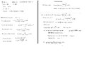
I started (draft design on paper) with flyback DCM topology.

1) ICE3BR0665J controller, 65 kHz, 0.65Ohm RDSon
2) VS-48CTQ060PbF output Schotky diode – the best in class with Vf=~0.5 voltage drop at 10A
3) Output caps before LC filter: 4pcs of Nichicon PW 1500 uF, 16V (1600 mA rms rated)
4) Transformer core EFD-25, Lprim=219 uH, turn ration n=Prim/Sec=10.5


My problems are:
1) I don’t know how to make the efficiency around 83 % staying in DCM and not using synchronous rectification.
2) To make output ripple current lower – because high ripple current makes me to use three caps before LC filter.

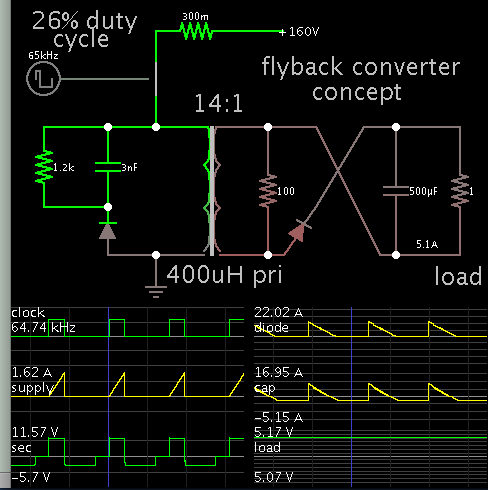
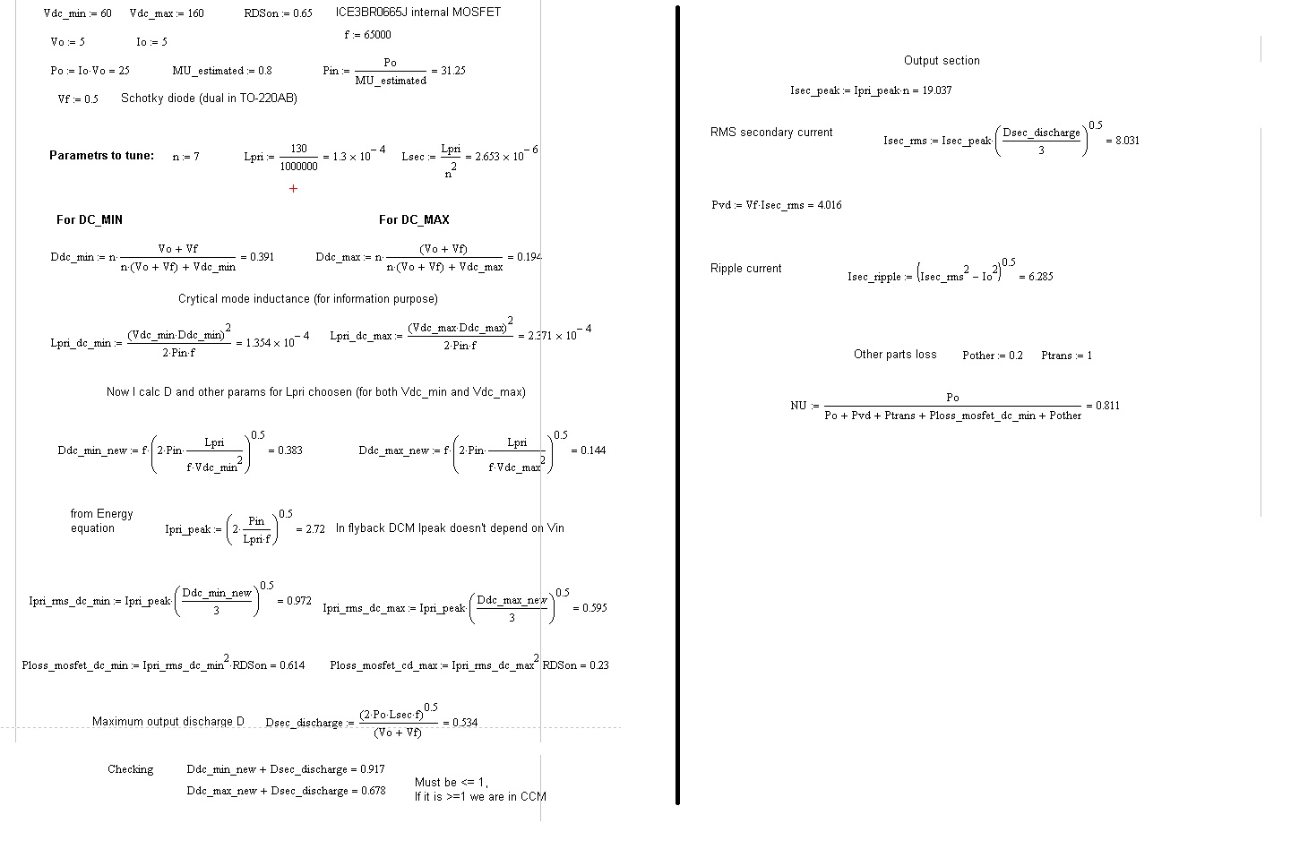
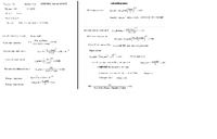
I attached my calcs.
I would like you (people) to check this calcs and give me advise how to minimize ripple current and increase efficiency of this flyback.


Thank you


Attachments

  • calcs.jpg
    calcs.jpg
    130.6 KB · Views: 114

I like to experiment with simulations. Your specs appear to work for 60V supply. I suppose you plan to reduce duty cycle for 160V supply? It appears that my simulation shows obstacles with 160V supply. When I reduce duty cycle it causes very large current spikes through the primary.

Question: Did you also make a design for 160V supply? You may need to change transformer parameters (step-down ratio, primary Henry value). As an alternate, make your switching frequency adjustable.

Most likely you'll use some middle values to design your transformer.

4pcs of Nichicon PW 1500 uF, 16V (1600 mA rms rated)

My simulation has 500uF which allows 1 or 2 percent ripple. It must handle current pulses as high as 30A. A gang of several capacitors is a good idea to share the burden, perhaps more than 4 pieces as your specs indicate.
 

>>Did you also make a design for 160V supply?
No I didn't. Was straight inside 60V problem.
It is not obvious what you are saying to me, because I can not do calculations right now. I will do calculations for my fixed Lpri=219uH and Vmax=160v tomorrow.

>>Most likely you'll use some middle values to design your transformer.
Please explain.


>>My simulation has 500uF which allows 1 or 2 percent ripple.
What simulation are you talking about?


I would appreciate if you could recommend a PWM controller with integrated MOSFET (similar to ICE3BR0665J RDSon~0.65Ohm) but with more comprehensive functionality (programmable UVLO, OVLO, shutdown pin - for output overvoltage functionality). Of course I can do it with ICE3BR0665J, but integrated solution is better. I have spent many hours looking for such IC, all of them were with RDSon~2ohm, or they lack CS pin, what is very important for me to program over-current functionality.
 

Here is my simulation for supply 160V. If it was unchanging we might select a step-down ratio of 20:1. But since supply voltage varies, we consider a compromise somewhere between 20 and 10.5. A suitable value appears to be 14:1.


The values appear to work for a range of supply voltage down to 60V. Duty cycle above 50% should be okay, since the second half of the cycle still has sufficient time for current to drop to zero.

The smoothing capacitor is 500 uF. Ripple voltage 2%. Notice it is exposed to large bursts of current (nearly 20A).

A suitable snubbing network is shown.

The 100 ohm resistor is unnecessary. It is there to measure secondary output V.
 

Here are two calcs for both dc_min and cd_max:
For L=400uH and n14
For L=130uH and n6

In first case I am out of DCM. In second case the duty cycle at 160V seems too low (maybe or maybe not).

What do you think, where should I stay?


I Don't have the time to go thorough all the calculations, but I'm going to describe what works for me.

I perform all calculations on an Excell spreadsheet, on which each individual subcircuit has its power loss calculated.
Then on my first round of calculations, I inspect which subcircuit has the highest loss, and focus my attention there.

Let's say for the sake of argument, that it is the snubber. I then tweak the snubber components to reduce losses, but some tradeoffs will occur. I.e, the Mosfet Vds(max) may be exceeded.

Then I look at a different, higher Vds Mosfet. Most likely, to remain in an approximate price range, it will have a higher Rds(on).
Calculate the new snubber and Mosfet losses, and compare with the previous revision to determine if total converter losses are now lower.

You may play around with other parameters, such as switching frequency.

There may be times, on which you will find that the only way to significantly reduce losses is to go to larger (read: higher priced) components.

That is the nature of electronic design. No circuit is optimized on the first attempt.
 

i would use the lowest voltage (and therfore low vf) schottky you can, and to do that, arrange the flyback so that the on-state voltage reflected to the diode is as small as possible, so do this by arranging the turns ratio accordingly. Have a good rc snubber across the schottky so it doesnt get overvoltage spiked.

- - - Updated - - -

Also, what is the 60-160v supply?..is it from battery?
 

Thank you guys for your answers.
I forgot to say that I am not very experienced in flybacks. Had few projects, mostly with good referance designs from IC producers.

The supply voltage is 85 V. That is for railroad. 4A charger for mobiiile devices.
Should be I afraid of CCM mode with ICE3BR0665J?

I don't need very fast response to load change in this project. No overshoot of course, but slow reaction is ok here
CCM will give extra percents to efficiency record.
 

thanks, whats the range of voltages over which the flyback is expected to continuously work if it sees that vin for long periods?...presumably the 160v is just a transient?
You need to use low as poss vf schottky to increase efficiency...and that is done by making voltage reflected from pri to sec as low as poss....remembering spikes.
 

The leakage inductance of the transformer would effect your whole performance. Try to reduce it if you would make the transformer by yourself.
 

yes, do interleaved winding...as in app note 18 by power integrations
 

Treez has something there with power integrations. Their website must have a hundred power supply designs as well as general design advice. They may have the design already done.
 

I have decided to start with CCM mode flyback. Infineon (ICE3BR0665J) has few APPnotes for CCM design.
Transformer interleaved winding means a lot in reducing Leakage inductance - that what I know for sure.

Power Integrations made a lot in popularizing Flybacks. But their ICs (TOP series) are voltage mode and have high enough RDSon.
I have designed several 12V flybacks based on TOP and they have been working fine as LED CV power supplies (in DCM mode only) since 2009.

Thank you all.
 

Status
Not open for further replies.

Similar threads

Part and Inventory Search

Welcome to EDABoard.com

Sponsor

Back
Top