shineqi
Member level 1
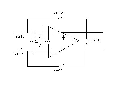
sample and hold design
I desinged a sample hold circuit for adc.
If I input 1V vpp, I cannot get 1v vpp from output.
But if I input 500mv vpp, I can get correct sampled 500mv vpp from output.
What is the reason caused this problem?
Not enough gain or not enough output swing or others?
BTW: how to simulate the trans gain to OTA and how to simulate output swing?
Thanks