Continue to Site

Welcome to EDAboard.com

Welcome to our site! EDAboard.com is an international Electronics Discussion Forum focused on EDA software, circuits, schematics, books, theory, papers, asic, pld, 8051, DSP, Network, RF, Analog Design, PCB, Service Manuals... and a whole lot more! To participate you need to register. Registration is free. Click here to register now.

Mystery Colors on the Si die

Status
Not open for further replies.

tinker1965

Newbie level 4
Joined
Dec 16, 2019
Messages
7
Helped
0
Reputation
0
Reaction score
0
Trophy points
1
Activity points
69
Came across an interesting picture today. Can anyone shed the light on why some diffusions on this die have different colors after a long HF etch? All of the oxide should have been etched away at this point. Note a loose poly gate at the BR corner
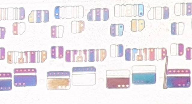
Capture.PNG
 

My guess would be diffraction of the light in the thin layers. Much like the reflection off a CD/DVD can split light wavelengths like a prism.

Brian.
 

thin film interference


1595342334406.png


drawing shows how light behaves to get to your eye and from this can determine what you see

when light goes from one medium to next, it refracts at the interface (snell's law)
it also reflects at the interface.

if the index of refraction of the new medium is greater than the index of refraction of the
original medium, the reflection picks up a 1/2 wavelength shift

if the index of refraction of the new medium is less than the index of refraction of the
original medium, the reflection does not pick up a 1/2 wavelength shift

combining the effect of the reflection with the path of ray 2 being twice the thickness
of the film longer than the path of ray 1, we get a relationship between the thickness
of the film, the wavelength of the light

to simplify the math, assume the incidence is perpendicular to the interface so we do not need snell's law

then 2t +(1/2 wavelength shift, if needed) = integer number of wavelengths of light in the medium gives constructive interference
while 2t +(1/2 wavelength shift, if needed) = (integer +1/2) number of wavelengths of light in the medium gives destructive interference

the different colors are therefore related to the thickness of the film and any underlying material
some colors are constructively interfered, so we see that color
some colors are destructively interfered, so we see do not that color
 
Thanks everyone for the input! I understand how thin films, e.g SiO2 will have different colors depending on thickness. I guess I did not phrase the question clearly, what I meant is:.
What kind of thin film could possibly be there to produce that kind of coloring? SiO2 has been etched away, unlikely that some still remained. Or does it look more like Ti Silicide or TiN over TiSi2?
 

it depends on the thickness of the film and the relative values of the indices of refraction
 

Silicide would only be in the source, drain regions
(salicide) and maybe the gate if it gets silicided
as well. It would not be the wide variety of colors,
and as it's really entrained in the silicon (and maybe
poly) it would be a uniform discoloration if anything.

Etching can be biased electrochemically by junctions
(decorating N or P type preferentially) but I have not
ever seen such a variety of colors on what look to be
fairly uniform devices.
 

Colors do only appear on top of source& drain (S/D). Both n+ and p+ areas are randomly affected. Whatever gives color is in between S/D Si and M1 metal, closer to S/D Si. Must be some sort of a barrier layer right on top of S/D
Not sure if that process even used silicide, if it did, TiN would most likely be right on top of it.
 

how consistent is the deposition before the "...long HF etch?"
how consistent is the "...long HF etch?"

small variations in the thickness of the last thin film layer and
some effects from snell's law (the incoming light is not perpendicular
to the interface) may account for variations in color from item to item
and in variability of color within an item. (last item in lower right)
 

I took another look and only p+ areas are showing colors, n+ seems to be unaffected. And only some of the p+ areas are colored (every single S/D on the picture above is p+). So it is not salicide.
Etching in HF for several hours would have taken care of all inconsistencies.
Whats left is either etching very very slowly, or is it possible p+ areas somehow grew a thin layer of oxide during DI water rinse or after exposure to air? doubt it would oxidize enough to show colors
 

Status
Not open for further replies.

Part and Inventory Search

Welcome to EDABoard.com

Sponsor

Back
Top