Welcome to our site! EDAboard.com is an international Electronics Discussion Forum focused on EDA software, circuits, schematics, books, theory, papers, asic, pld, 8051, DSP, Network, RF, Analog Design, PCB, Service Manuals... and a whole lot more! To participate you need to register. Registration is free. Click here to register now.
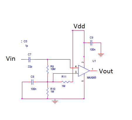
I wonder whether this is really asking for the frequency at
which the kooky input network starts to allow output toggle
instead of sitting there doing nothing.
Not that I know all about what causes latch-up, but I understand it can occur when the input terminals are exposed to a voltage outside the supply rails. In your schematic this might happen, if the input receives a sufficiently high frequency, at sufficient amplitude. (Slower frequencies are blocked by the high-pass filter, formed by the RC network.)
A low-pass filter is at the op amp's lower input. This complicates things, of course.
I don't think anything about latchup sensitivity can be
deduced from the info provided. Physical design features
are largely what matter, one part can be made to latch up
with a few mA of pin-substrate current and another, never
at a hundred mA.
I think it's a mis-expression of the real question, whatever
that might be.
This site uses cookies to help personalise content, tailor your experience and to keep you logged in if you register.
By continuing to use this site, you are consenting to our use of cookies.