Continue to Site

Welcome to EDAboard.com

Welcome to our site! EDAboard.com is an international Electronics Discussion Forum focused on EDA software, circuits, schematics, books, theory, papers, asic, pld, 8051, DSP, Network, RF, Analog Design, PCB, Service Manuals... and a whole lot more! To participate you need to register. Registration is free. Click here to register now.

MOS used as a capacitance

Status
Not open for further replies.

Junus2012

Advanced Member level 5
Joined
Jan 9, 2012
Messages
1,552
Helped
47
Reputation
98
Reaction score
53
Trophy points
1,328
Location
Italy
Activity points
15,235
Dear friends

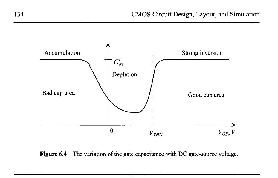
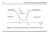
I have used the MOS as a capacitor. I am running it under the saturation strong inversion region.

I have attached you this picture from Jakob Baker book. He told that in order to use the MOS a capacitor it must work in the strong inversion because it has less or no voltage dependency as shown in the graph.
However, the grph also shows the same stability in the accumulation region but the author told it is not good region to work as a capacitor. he didn't say why

But I am saying why ????

Please also to tell me the differences and the disadvantages between the MOS capacitor and the two parallel plate capacitor

Thank you in advance


The device is turned off, there is no channel. so yes you will have a constant cap but the cap is now a Gate to Body cap, which is very small. essentially like having a small strip of poly over nothing(think parasitic cap). for the device to act as a good cap, you need to make use of the very very small gap between the gate and the channel (the very think fox layer separating the two). to do this you need the device on, but as mentioned if the device is on and in subthreshold region the cap is heavily dependent on Vgs.
-Pb
 

But you see the capacitance in the accumulation region has the same value from the strong inversion, I am not iterested in the conduction, the important thing for me the capacitance value......... unless if this wrong


The device is turned off, there is no channel. so yes you will have a constant cap but the cap is now a Gate to Body cap, which is very small. essentially like having a small strip of poly over nothing(think parasitic cap). for the device to act as a good cap, you need to make use of the very very small gap between the gate and the channel (the very think fox layer separating the two). to do this you need the device on, but as mentioned if the device is on and in subthreshold region the cap is heavily dependent on Vgs.
-Pb
 

That is cox. the capacitance of the oxide between the gate and the channel.
But I may be wrong on my assumptions, will look into this

- - - Updated - - -

I cant find any claim against this, in fact the accumulation region appears to be the best between low frequency and high frequency. I think for my own curiosity now I will have to sim this in an impedance divider to see how a nmos whos gate is at say .2v and ds is tied at supply and how that stacks against a nmos gate at 1v and ds tied to ground. I will let you know of my results.
-Pb

- - - Updated - - -

Ok so this basically answers your Question. Turns out I was right though I cant explain it. The saturation cap is the largest and fairly constant over vgs. subthreshold voltage is 2nd largest and all over with vgs. and accumulation is constant with cgs but lower cap value.
what i did were a series of frequency sweeps. Grailcap is mosfet connecting its drain/source to ground, and sweep vgs of 1V to 1.6V, prailcap is drain/source to 1.8V and sweep vgs from -1.6V to -1V , sgrail I keep drain/source at ground and sweep vgs from .2 to .8V
moscap.png
hope this helped,
-Pb
 
Last edited:

-points at picture- both regions are constant across voltage, buuut the device whos vgs >vt has a much larger gate capacitance. in this case about 3x.
 

if you again see the graph, both they have the same value

thank you for your reply

-points at picture- both regions are constant across voltage, buuut the device whos vgs >vt has a much larger gate capacitance. in this case about 3x.
 

Im referring to my simulation of the three regions, they do not have the same value, they may have the same cox, but not the same Cgs/Cgd/Cgb caps
 

I am only talking about cox

Im referring to my simulation of the three regions, they do not have the same value, they may have the same cox, but not the same Cgs/Cgd/Cgb caps
 

lets consider NMOS. In accumulation your gate voltage should be lower than source potential - so the holes are attracted to the gate and so the capacitor is created between the poly of the gate, positive charge in channel which are divided by oxide. Co that is why the capacitance value is the same as in strong inversion - where instead of holes the channel is flooded with negative charge electrons.
Now - what is better contact for you N+ to conduct holes or N+ and electrons? How will you generate the negative bias? (it is surely possible but then I ask Why if we don't have to?)
 

The figure is also from Baker's book.

In accumulation, one side of the cap is connected to substrate and
there's a significant resistance in series with cap.
In strong inversion, one side of the cap is connected to diffusion via inverted layer and
the series resistance is very small.

The moscap in strong inversion region is better than in accumulation region.
 

Attachments

  • moscap.bmp
    636 KB · Views: 61
Yes, this is the real answer
The figure is also from Baker's book.

In accumulation, one side of the cap is connected to substrate and
there's a significant resistance in series with cap.
In strong inversion, one side of the cap is connected to diffusion via inverted layer and
the series resistance is very small.

The moscap in strong inversion region is better than in accumulation region.
 

Status
Not open for further replies.

Part and Inventory Search

Welcome to EDABoard.com

Sponsor

Back
Top