Continue to Site

Welcome to EDAboard.com

Welcome to our site! EDAboard.com is an international Electronics Discussion Forum focused on EDA software, circuits, schematics, books, theory, papers, asic, pld, 8051, DSP, Network, RF, Analog Design, PCB, Service Manuals... and a whole lot more! To participate you need to register. Registration is free. Click here to register now.

Matching Biasing circuit to the core amplifier

Status
Not open for further replies.

Junus2012

Advanced Member level 5
Joined
Jan 9, 2012
Messages
1,552
Helped
47
Reputation
98
Reaction score
53
Trophy points
1,328
Location
Italy
Activity points
15,235
Dear friends,

I am presenting an issue of layout matching between the core amplifier circuit to the biasing circuit,

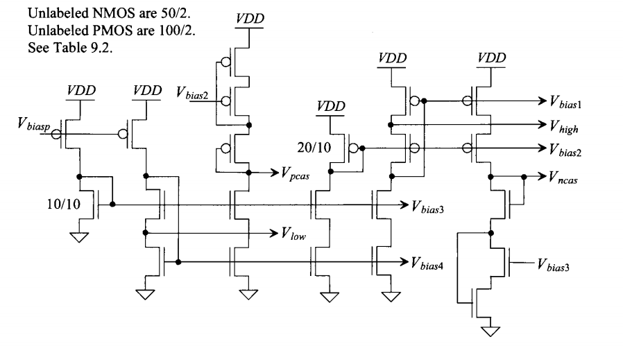
The biasing circuit is designed in separate cell, as the one shown below
bias1.png


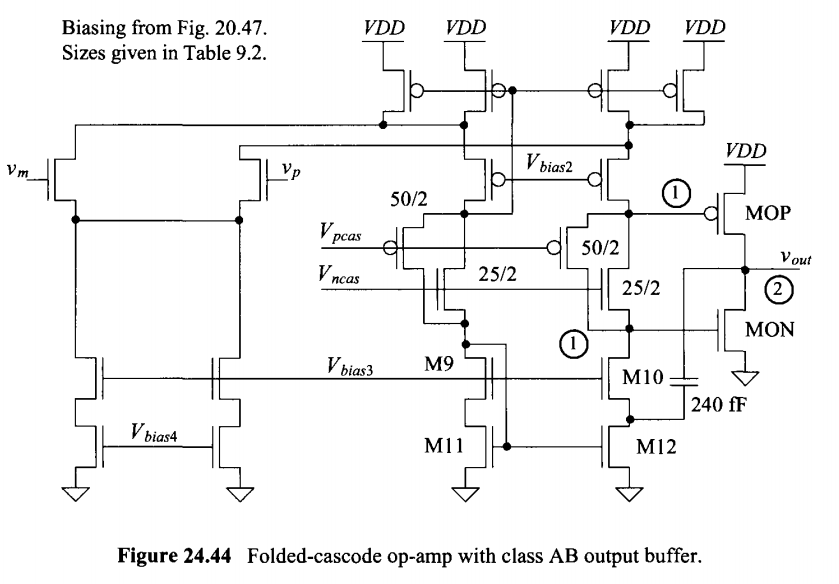
The core amplifier shown below is also designed in different cell, as the one shown below
bias2.png


My concern is that, how we would be assure that vbias voltages (vbias1, vbias2, vbias3, vbias4, vncas, vpcas) from the biasing circuit will be matched to the amplifier.
In the same time, thinking to build the biasing circuit in the same amplifier cell and matching them during layout is not easy solution for two reasons because design with hierarchy is more preferable and because the biasing circuit is biasing other different circuit. Therefore if we embeds the biasing circuit with the amplifier core will require to design and biasing circuit for every sub block in electronic system design.

Thank you very much
Best Regards
 

Introducing hierarchy is for your organization of the design and better readability, etc. Physical placement, although it follows the hierarchy organization doesn't really care about hierarchy in the drawn schematics. What I mean is that for example you can physically place two transistors such that they abut each other but still come form different hierarchical blocks in the schematics.
This being said, it is a good practice to keep transistors generating the bias voltages close to the transistors receiving those bias voltages and preferably in the same diffusion (OD). You can, for example add same size dummies between the generating devices and the receiving devices to cover the distance but that distance should not be excessive. Maybe worth of no more that a few dummies.
A good practice is to distribute currents, instead of voltages for biasing stuff and then from those currents generate bias voltages locally. Thus, you can have one master bias block from which you send bias currents to local bias blocks. In this respect, going to your first circuit, it is much better not to get the voltage Vbiasp, but to get the current that goes down to the NMOS diodes.
 
Dear Suta

Thank you very much for your reply and nice explanation,

I would prefer to go on your second solution that is biasing the circuit locally by distributing bias current from the main biasing circuit, I understand it like this way and please correct me if I am wrong,

1. Since the current has no problem of dropping (rout R in series), hence the current generated from the biasing circuit can reach safely to any local place in the core amplifier or any other circuit. See please the beta multiplier biasing circuit below

bias3.png


Where Vbiasp will be converted to current by means of mirror

2. from the reference current we construct local biasing circuit to gene vbias1.....vbias4 and this these local biasing voltage circuits should be matched to the amplifier core

Thank you once again
 

Since the current has no problem of dropping (rout R in series), hence the current generated from the biasing circuit can reach safely to any local place in the core amplifier or any other circuit.
This is wishful thinking. Gate leakage in process with gate thickness of 1-2nm is high enough to deteriorate operating point of bias circuit or receiver circuit.

Matching. In some process spatial mismatch is small and in order of few mV/mm of distance (threshold voltage), while for other matching is lost after 10um distance between devices.

PSRR is another aspect. By adding cap to internal node of reference loop, it gain drops faster and worst case PSRR become poor. Moreover, finite Intrinsic gain of transistor results with kickback of signal on gate voltage. Now, you can imagine what happens if you have single voltage bias, which couples all circuits together.

In books, papers bias circuit and core circuits are shown separately for simplicity of reading.
 
Dear friends,

Thank you for your help

I am now designing the circuit based on local biasing scheme which will be matched to the amplifier core, I will match the local the local biasing circuit transistors to the core amplifier transistors, not only simple matching by putting it just in near distance, but by interdegitizing them in the matched array of the core amplifier transistors...... As a confirmation to your notes and as find this in the book of "The Art of analog Layout" as given in the image below (notice please the matching note on the lift of the circuit)

bias.png


Thank you once again for your help
 

Status
Not open for further replies.

Part and Inventory Search

Welcome to EDABoard.com

Sponsor

Back
Top