Continue to Site

Welcome to EDAboard.com

Welcome to our site! EDAboard.com is an international Electronics Discussion Forum focused on EDA software, circuits, schematics, books, theory, papers, asic, pld, 8051, DSP, Network, RF, Analog Design, PCB, Service Manuals... and a whole lot more! To participate you need to register. Registration is free. Click here to register now.

LTSpice Simulation

Status
Not open for further replies.

KronosX

Newbie
Joined
Oct 13, 2022
Messages
3
Helped
0
Reputation
0
Reaction score
0
Trophy points
1
Activity points
22
Hello,

I need help in plotting the output current vs the drain voltage from 0 to 10 Volts.
I'm not sure what am I doing wrong with my simulation.
I added the width and length of all transistors and set the model to match the parameters specified.
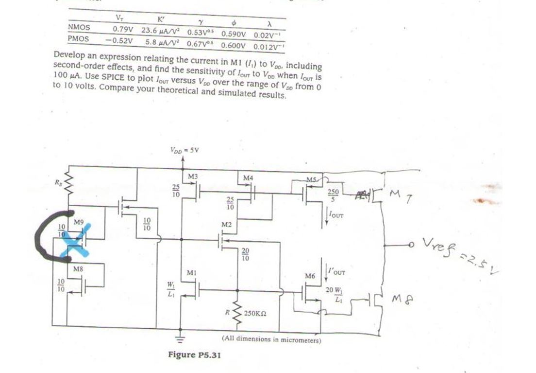
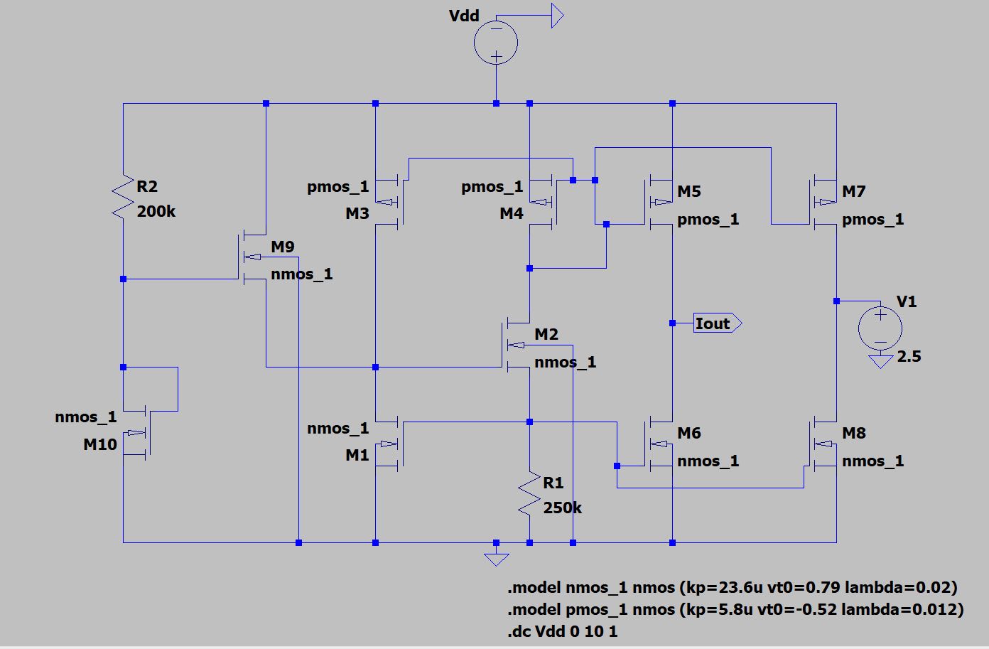
Project Description.JPG


Schematic.JPG


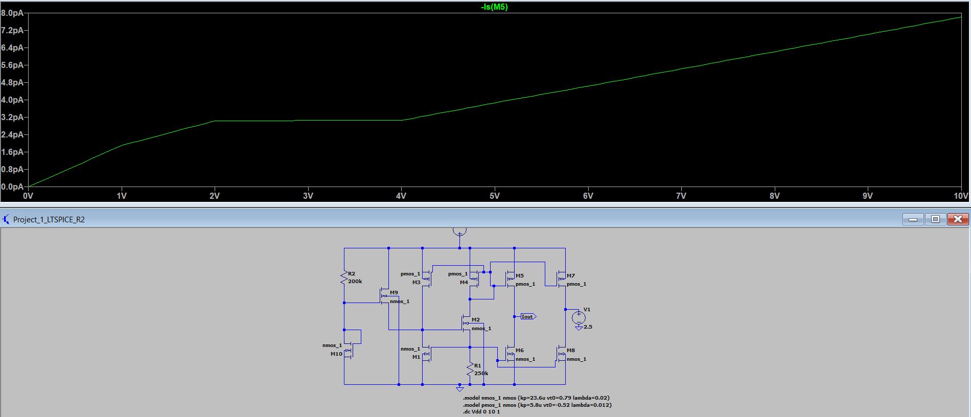
Simulation.JPG
 

Hi,

Looking at the diagrams, a few things I have noticed:

*You have substituted MOSFETs for JFETs.
*Iout and I'out are two different variables but you have tied them together and given them the name Iout.

Correct these, try again and let us know the result.
 

You have substituted MOSFETs for JFETs.
Don't think so. All transistors have insulated gate, no JFETs. Just strange circuit drawing style. Substrate connection is only explicitely shown for transistors with floating source.

Fault is measuring difference current Iout - Iout' instead of Iout, as stated.

Don't know why M9 has been removed.
 

Hello,

I substituted jfets for mosfets and used "COM" to split Iout and I'out. Using two different output ports was giving me no current.
I'm still not satisfied with the results since they should match my theoretical results. Any ideas?

Thanks.

Simulation.JPG
 

The problem starts at the bias node R2 / M10, which the follower
NMOS M9 soaks up with its VT so nothing left for the rest
(M1, M2).

Try stacking another nmos between M10 and GND.
 
  • Like
Reactions: d123

    d123

    Points: 2
    Helpful Answer Positive Rating
Don't think so. All transistors have insulated gate, no JFETs. Just strange circuit drawing style. Substrate connection is only explicitely shown for transistors with floating source.
Yes, I have realised it. The parameters in the questions are for MOSFETs.
--- Updated ---

Hello,

I substituted jfets for mosfets and used "COM" to split Iout and I'out. Using two different output ports was giving me no current.
You're basically still having M5 and M6 connected in series.
You might need to connect a suitable load to do the current measurement.
 
Last edited:

Also, considering the parameters, how have you considered W/L, phi, and gamma?
 

Status
Not open for further replies.

Part and Inventory Search

Welcome to EDABoard.com

Sponsor

Back
Top