Reschak
Newbie level 6
Hi all
Got some screenshots attached for a low noise amplifier using an ATF-34143 FET from avago. The objective is to create this amplifer on a PCB with the following specs:
1. Unconditional stability across 0-18 GHz
2. S21 > 15dB between 1.5-1.6 GHz
3. noise figure < 1dB between 1.5-1.6 GHz
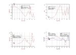
The circuit performance pic shows the K factor (StabFact1) and mu factors for stability. Everything seems fine until about 10 GHz when everything goes wild.
I'm mostly concerned about the stability dip at 15 GHz. Need to rectify this without damaging the noise or gain by too much. I've tried adjusting the component values and microstrip lengths by can't find the root of the problem. It's probably to do with the R L C feedback loop, which is needed for low frequency stability. I don't know much about oscillation but could that be the cause?
also included is a preliminary layout because the microstrip lines and vias are also factors in the stability. TL1 and TL13 are 50 Ohm lines with widths 1.5 mm and lengths 5 mm to give a sense of the scale.
Any and all help is appreciated! Any tips or improvements also very welcome
thanks


**broken link removed****broken link removed****broken link removed**
Got some screenshots attached for a low noise amplifier using an ATF-34143 FET from avago. The objective is to create this amplifer on a PCB with the following specs:
1. Unconditional stability across 0-18 GHz
2. S21 > 15dB between 1.5-1.6 GHz
3. noise figure < 1dB between 1.5-1.6 GHz
The circuit performance pic shows the K factor (StabFact1) and mu factors for stability. Everything seems fine until about 10 GHz when everything goes wild.
I'm mostly concerned about the stability dip at 15 GHz. Need to rectify this without damaging the noise or gain by too much. I've tried adjusting the component values and microstrip lengths by can't find the root of the problem. It's probably to do with the R L C feedback loop, which is needed for low frequency stability. I don't know much about oscillation but could that be the cause?
also included is a preliminary layout because the microstrip lines and vias are also factors in the stability. TL1 and TL13 are 50 Ohm lines with widths 1.5 mm and lengths 5 mm to give a sense of the scale.
Any and all help is appreciated! Any tips or improvements also very welcome
thanks


**broken link removed****broken link removed****broken link removed**