Continue to Site

Welcome to EDAboard.com

Welcome to our site! EDAboard.com is an international Electronics Discussion Forum focused on EDA software, circuits, schematics, books, theory, papers, asic, pld, 8051, DSP, Network, RF, Analog Design, PCB, Service Manuals... and a whole lot more! To participate you need to register. Registration is free. Click here to register now.

LM5116 buck converter problem - not working

Status
Not open for further replies.
Hi,

Sorry here was a misunderstanding.
You:
with ground plane on both sides,
Me:
single sided GND plane is sufficient

I meant GND plane on one side.
But components and other signal on the other side.
So: double sided pcb, but gnd plane only on one side.

****
On your pcb it seems a lot of parts are connected on one side only. C16, C17...C22 for example.

Klaus
 

Hi,

So: double sided pcb, but gnd plane only on one side.

Klaus

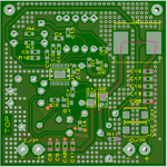
Done with the changes. Kindly check it. But I have given ground plane on both sides. Will it cause any trouble?
 

Attachments

  • board bottom side.png
    board bottom side.png
    99.1 KB · Views: 122
  • board top side.png
    board top side.png
    118.8 KB · Views: 145
  • PCB layout.png
    PCB layout.png
    139.2 KB · Views: 272

Hi,

Datasheet says:
***
In a buck regulator, the primary switching loop consists of the input capacitor, MOSFETs, and current sense
resistor. Minimizing the area of this loop reduces the stray inductance and minimizes noise and possible erratic
operation. The input capacitor should be placed as close as possible to the MOSFETs, with the VIN side of the
capacitor connected directly to the high-side MOSFET drain, and the GND side of the capacitor connected as
close as possible to the low-side source or current sense resistor ground connection. A ground plane in the PC
board is recommended as a means to connect the quiet end (input voltage ground side) of the input filter
capacitors to the output filter capacitors and the PGND pin of the regulator. Connect all of the low power ground
connections (CSS, RT, CRAMP) directly to the regulator AGND pin. Connect the AGND and PGND pins together
through to a topside copper area covering the entire underside of the device. Place several vias in this underside
copper area to the ground plane.
***
5116.png
***
I´ve drawn the two switching loops in red and magenta.
--> I don´t think you "minimized the area".
* You could shorten the distance of C8..C11 to Q1.
* Shorten the distance Q2 to L1.
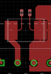
* And shorten the GND path from C16..C20 back to C8..C11. (just by placing vias directely to C8..C11)

Additionally:
* Place two vias each to GND directely to C2 and C14. Don´t connect the GNDs at the top side.
* Your R11 is very small. It needs to be able to carry a lot of switching current. (expect > 10A) Check size.
* Please connect R6 and R7 with independent wires directely to R11.

There may be other issues..
But it is much better now, and I expect that it works now. (As long as you took care about inductor and capacitor selection guidelines)
Many vias are totally useless. Especially those at the top edge of the PCB. But they won´t harm

Klaus
 

Hi,

* Please connect R6 and R7 with independent wires directely to R11.

Klaus

I dont get it. Only R6 gets connected to R11, while the other end of R7 and R11 are grounded. What should i change in this?
 

Hi,

R6 and R7 are the (precision) paths for current measurement.

--> connect R6 with a wire directely to the one pad of R11.(The wire should not be used for other connections. Just R6 to R11)
--> connect R7 with a wire directely to the other pad of R11.(The wire should not be used for other connections. Just R7 to R11)

I know R7 is connected to GND... but it is the sense path for current measurement.
On R11 there are pulsed currents causing GND bounce. So, for precise current measurement don´t connect R7 to the GND plane, but connect it to the R11 pad. (And the R11 pad is connected to GND plane)

like this:
5116_cm.png

Klaus
 

Hi,

R6 and R7 are the (precision) paths for current measurement.

--> connect R6 with a wire directely to the one pad of R11.(The wire should not be used for other connections. Just R6 to R11)
--> connect R7 with a wire directely to the other pad of R11.(The wire should not be used for other connections. Just R7 to R11)

Klaus

Done, as per your suggestion.

The i/p path C8 to Q1 and o/p path Q2 to L1 is shortenend. R6, R7 and R11. Is it ok?
 

Attachments

  • board bottom side.png
    board bottom side.png
    93.2 KB · Views: 77
  • board top side.png
    board top side.png
    95.4 KB · Views: 101
  • PCB layout.png
    PCB layout.png
    127.4 KB · Views: 101

Hi,

.. It will do...

...(just by placing vias directely to C8..C11)...
Vias are still missing.

Klaus
 

Hi,

Vias are still missing.

Klaus

Done with vias for C8-C11 as like in C16-C20

- - - Updated - - -

All done.? Is the board good enough to be outsourced for fabrication..?
 

Attachments

  • vias done.png
    vias done.png
    78.5 KB · Views: 103

Hi,

to be honest.. it is not perfect.

But it should work, as far as I can see.

***
I´m still worried about the size of L1. What type is it? Datasheet?


Klaus
 

Hi,

to be honest.. it is not perfect.

But it should work, as far as I can see.

***
I´m still worried about the size of L1. What type is it? Datasheet?


Klaus

:cry::sad:

Well, i've given the bigger pad to accomodate any type of inductor that gives me the outupt.

ADDED:
Please tell the way to make it perfect.
 
Last edited:

I've completely soldered 9 board. Out of 9, only 5 boards work good. When the input varies from 14V to 90V, the board outputs 12 to 12.8V.

For the remaining 4 boards, there are some problems. The output keeps on increasing with an increase in input voltage and then the LM5116 fuses out.
Also there is a severe humming sound when the input voltage increases beyond 16V.

I have used the same components for all the 9 boards. What might cause such problem?
 

But got no informations from you.

Sorry for not mentioning about the inductor.

I used two types of inductors.
1. The inductor part number is ETQ-P6F3R2HFA from digikey. (couldn't find the datasheet)
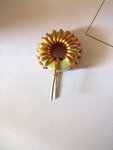
2. I've included the picture of the other inductor (10uH/5A).

10uH inductor.jpg

I got the output using the 1st inductor. Now also i'm getting the output, but it does not stand stable in 12v. The o/p voltage increases with increase in the i/p voltage and then the LM5116 fuses out. I use the same components for all boards. (I get a beep sound with connectivity mode between the + and - of the LM5116. If i replace the IC with a new one, again it works.)
 

Hi,

The first one seems to be a storage choke, but the second seems to be for RF suppression.
Read datasheets. Just try will result in fails.

Also calculate:
What inductance values did you calculate? With what values?
Inductance and current. RMS, ripple and saturation current.
LM5116 datasheet section 8.2.2.2.

Klaus
 

Hi

Please find the schematic in the page.11 of the pdf. Used exactly the same components, except for the inductor.
 

Attachments

  • lm5116-evaluation board.pdf
    362.4 KB · Views: 121

Status
Not open for further replies.

Similar threads

Part and Inventory Search

Welcome to EDABoard.com

Sponsor

Back
Top