- Joined
- Jan 22, 2008
- Messages
- 52,422
- Helped
- 14,749
- Reputation
- 29,780
- Reaction score
- 14,101
- Trophy points
- 1,393
- Location
- Bochum, Germany
- Activity points
- 298,107
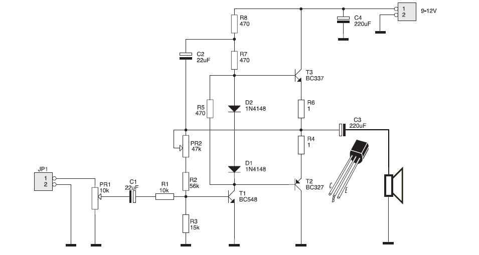
I guess, it would be interesting to analyze the exact circuit.
Follow along with the video below to see how to install our site as a web app on your home screen.
Note: This feature may not be available in some browsers.


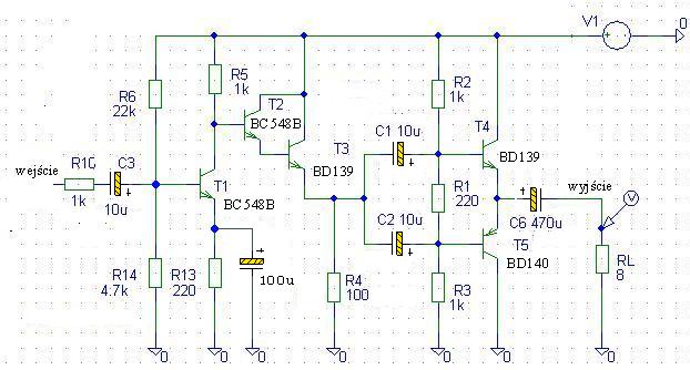
Yes, the DC path is provided by R9.does the C3 is correctly placed
R9 provide the the DC path but also determines close loop voltage gain.Thanks for your reply, well I thought that R9 was here to make the feedback not to provide the DC from the output of the amplifier...
This book is goodMaybe I would have to study again transistor basics; does anyone know a good book(s) for polarisation/multiple stages design and feedback theory of transistor stages ?