Continue to Site

Welcome to EDAboard.com

Welcome to our site! EDAboard.com is an international Electronics Discussion Forum focused on EDA software, circuits, schematics, books, theory, papers, asic, pld, 8051, DSP, Network, RF, Analog Design, PCB, Service Manuals... and a whole lot more! To participate you need to register. Registration is free. Click here to register now.

Inside linear voltage regulators

engr_joni_ee

Advanced Member level 3
Joined
Nov 3, 2018
Messages
750
Helped
2
Reputation
4
Reaction score
4
Trophy points
18
Activity points
6,229
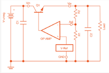
I am trying to understand the functionality of linear regulators. I have attached the fundamental circuit of linear regulator.

Can someone please explain how does the circuit work ?

I am also wondering where the V-Ref comes from ? Consider two following two cases.

Vin = 5.0 V
Vout = 4.0 V
Iout = 1 A

Vin = 3.3 V
Vout = 2.5 V
Iout = 1 A

Would V-Ref be the same for both cases or not ?
 

Attachments

  • Untitled 611.png
    Untitled 611.png
    50.5 KB · Views: 56
Hi,

There is a mistake:
top line: left of Q1 it says "Vin" - this is correct. But right of Q1, it also says "Vin" --> it should be "Vout"

Thus I doubt the circuit is from a reliable source. --> always look at reliable sources, as there are:
* Semiconductor manufacturers
* universities
* reputable electronics designers
(but not from random web sites)

****
Functional description:
* Input capacitor C1,
* output capacitor C2
* power transistor Q1
* voltage reference VRef
* error amplifier OPAMP
* voltage divider R1, R2 as feedback to adjust the output voltage.

Basically it regulates VAdj to be the same as VRef.
If VAdj is too low, it increases the voltage on base_Q1, thus it increase VOut ... and vice versa.

****
Would V-Ref be the same for both cases or not ?
If you use the same regulator: yes.
A different regulator may have a different VRef.
To me this is a too general question at all. It´s like asking: do all people have same shoe size when driving different cars? --> same people will have same shoe size, different people will have different shoe size.

******

There are many different voltage regulators, with different internal and external circuit. Thus your schematic does not apply to all regulators.
As always: Read the datasheet - it usually has a functional description.

Klaus
 
I understand that if the Vout drops then the voltage divider V_ADJ also drops and will be smaller them V-Ref which means that there will be some output from the operational amplifier that is connected to the base of the NPN transistor.

But when the Vout is stable and the voltage divider V_ADJ is equals to the V-Ref then theoretically if Vin+ and Vin- are the same then the output of the operational amplifier is zero which means that the NPN transistor will not conduct, is that true ?
 
No, here is sim :

1708086399739.png


For varying Rload. The OpAmp output drives the fdbk R junction to be equal to Vref, in this case
3.3V.


Regards, Dana.
 
I think I am getting it now.

1- The linear regulator output voltage v_out is zero in the start.
2- The voltage divider voltage v_adj across R1, will also be zero which is connected to inverting input of the operational amplifier.
3- The v_ref is connected to non-inverting input of the operational amplifier.
4- The output of the operational amplifier will be high as vin+(v_ref) > vin-(v_adj).
5- The NPN transistor Q1 will conduct because the high output of the operational amplifier will turn on the the NPN transistor Q1.
6- Assuming the base to emitter voltage 600 mV (which is usually called drop out voltage in linear regulator).
7- The output voltage of the linear regulator start increasing that will also increase the voltage divider voltage v_adj across R2, which is connected to inverting input of the operational amplifier.
8- As the output of the linear regulator increase further, this will increase vin-(v_adj) compared to vin+(v_ref), causing the output of the operational amplifier low which will turn off the NPN transistor Q1.
9- The capacitor across the output load C2 will stabilize the output voltage through it's dis-charging during the time when NPN transistor Q1 is off.
10- As the output of the linear regulator start decreasing, this will lower the v_adj causing vin+(v_ref) > vin-(v_adj), which turn on the NPN transistor Q1 through the high output of the operational amplifier. This is how the linear regulator stabilize the output.
 
For varying Rload. The OpAmp output drives the fdbk R junction to be equal to Vref, in this case
3.3V. Note how OpAmp output is ~ 1 Vbe above Vout, to allow Transistor to supply load current.

The transistor never turns on and off when in regulation, as it supplies continuous load current.

Here is a case where 1V RMS ripple added to input, notice output barely moving (pay attention
to Y axis scaling)

1708087413827.png


Even the OpAmp with its ripple supply V has high PSRR that rejects the ripple from
appearing on its output. But thats a f(frequency) as the OpAmp starts running out
of G at higher freq which results in less ability to regulate the control loop. Most
datasheets have a graph of this (this is not the OpAmp I used, just a typical graph)

1708087829330.png


Regards, Dana.
 
Last edited:
Maybe the confusion is how the feedback amplifier works. It isn't true to say the output is zero when the inputs are the same, that only applies when the amplifier runs on positive and negative supplies and the input is zero referenced. In this situation, one input is the voltage reference and the output is also the same reference with some correction added. The correction voltage is a sample of the output voltage, suitably scaled with a potential divider so it matches the reference at the error amplifier inputs. If the output voltage drops, the scaled voltage drops and is then below the reference, the inversion in the error amplifier raises its output voltage and hence tries to compensate by bringing the output voltage higher again. It is a DC circuit with feedback, there is no charging and discharging capacitors as part of its operation except for when first powered up and minor changes as the regulation takes place.

Brian.
 
They use the principle that the inputs of an opamp (error amp) will become pretty much the same when there is negative feedback...like you get in an opamp integrator. (error amplifier).
Download the free LTspice and play with the attached simulation.
Playing is best. Good way to learn.
Take your understanding as it is...be accepting of it...then make some postulation by way of it...then test out your postulation on the sim.....better to test on the real hardware but such "Playing" takles too long if you always do it in real hardware.
 

Attachments

  • Linear Regulator.zip
    1.4 KB · Views: 41
VRef is almost always a bandgap core. Its form in old bipolar
technologies differs from what a CMOS-bandgap-trained
designer might expect. Crack open the oldest National linear
databook you can find, there will be reasonable detailed
schematics (though always lacking sizing info, you can get
that from microscopy).
 
Thanks for your comments. They are very helpful to me in understanding the internal components of the linear regulator. I also understand how they work together and how the output voltage is stabilized and what is the main reason for dropout voltage and heat dissipation.

Regarding V-ref, which is the internally generated in linear voltage regulator, you mentioned that "VRef is almost always a bandgap core. Its form in old bipolar technologies differs from what a CMOS-bandgap-trained designer might expect."

The concept of CMOS-bandgap core, is also true for voltage reference devices as well ? Usually voltage reference does not support large output current like linear voltage regulators.
 
In CMOS you will use an op amp to get the needed gain. Which is
not terrible for area, because lithography. But it adds its own mismatch
and frequency response terms.

In bipolar, older processes you have a much superior Early voltage
and your "amplifier" may just be a current mirror on the horns of
the bandgap ratio-pair.

But things are often "folded differently" as well, like you may see
the delta-Vbe developed on a segment of the feedback ladder
rather than in the pair tail (because freebie, not an extra and large,
if you're operating at low power, resistor.

Bipolar bandgap references can be done by bandgap or by the
often-available buried zener (if you have N+ sinker, you put a
P+ "top hat" on that and all the action is subsurface, free of
oxide interface traps and such to bother the low current reverse
characteristics with various drift mechanisms). If the reference is
+10V you are likely to see the zener approach.Gets tough or
impractical at 5V or under unless you want a buffered divider.
Which has been done, as has bare divider (now you need to know
that your attached load input current drifts insignificantly).

LT1009 is an interesting example of a bandgap folded neatly and
giving 2X the bandgap voltage by feedback.
 
Your block diagram is similar to the TL431 programmable Zener which uses a 2.5V Bandgap temp. compensated Vref.

The BG references were patented in 1971 by Bob Widlar and Robert Dobkin. Bob Pease had also written much about using them as a self-appointed Czar*.

The 3 Terminal LDOs use a 1.25V Bandgap constant voltage between Vout and Vadj, where fixed Vout use internal R ratio feedback and adjustable use external R feedback and no connection to ground except from external R shunt.


For lots of analog history There are 9 parts in this archive. (edit next link)
Bob_Pease_Lab_Notes_Part_1 : https://archive.org/details/Bob_Pease_Lab_Notes_Part_1/page/n19/mode/2up?q=Bob+Pease

Bob Pease , Sr. Designer National Semi 1990 1708194130395.png*
1708193717661.png


Now with modern FET, similar BG's are below 1V or 0.6V typ. and continue to improve in R&D with ~ 5ppm/'C with laser trimming.
 
I've never liked delta-VT references because most of my parts go
to radiation-exposed applications, which makes a mess of subthreshold
linearity (absent RHBD layout tricks, where these work) and induces
bias dependent VT shifts (which, nothing can save you from, at least in
continuous-time analog; chopping / zeroing, maybe).
 
I am still wondering about my question in post #10.

The concept of CMOS-bandgap core, is also true for voltage reference devices as well ? Usually voltage reference does not support large output current like linear voltage regulators.
Is that the question?

The reference circuit is always a low current part of either a reference IC or a voltage regulator.
The output current is just amplified by larger internal transistors for a regulator.
 

LaTeX Commands Quick-Menu:

Similar threads

Part and Inventory Search

Welcome to EDABoard.com

Sponsor

Back
Top