Continue to Site

Welcome to EDAboard.com

Welcome to our site! EDAboard.com is an international Electronics Discussion Forum focused on EDA software, circuits, schematics, books, theory, papers, asic, pld, 8051, DSP, Network, RF, Analog Design, PCB, Service Manuals... and a whole lot more! To participate you need to register. Registration is free. Click here to register now.

[SOLVED] Insertion Loss for power divider

Status
Not open for further replies.

belma1511

Junior Member level 1
Joined
Oct 17, 2013
Messages
18
Helped
0
Reputation
0
Reaction score
0
Trophy points
1
Activity points
126
Hello,

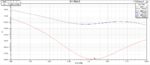
Currently I have a problem with the Insertion Loss parameter for my Wilkinson power divider. Its value is about -20dB which is way too low (expected is about -3dB). Can anyone have a look at my circuit and help me with this issue? The operating frequency is 5.5GHz and the substrate I used is FR4_epoxy (in HFSS).
View attachment Model.rar Izrezak.PNGIzrezak1.PNG
 

Does anyone have an idea? Please,it's urgent!
 

Do you have a resistor as lumped port as the rectangle between the legs or just metal? should be resistor with 2xZo. impedance of lines in branch of divider should be sqrt(2)xZo. lengths of branches should be 1/4 wave at frequency of interest. where is S11 minimum? please add plot of s11. FR4 is quite lossy but that sounds excessive.
 

I calculated the transmission lines' lengths and widths in Ansoft designer for the impedances 50Ω and 70.71Ω ( Z0=50Ω).
The resistor is simply determined as a impedance with 50 Ohm/square,100Ohm in total,no lumped port assigned.
Here is the plot of S11..as you can see the results are far from acceptable. Which substrat material would you suggest for this frequency range of 5.5GHz?
s11.PNG
 

try a wider sweep 1-10 GHz to see if anything jumps out. Rogers 5880 or duroid are better substrates. Also how high above the top of the substrate is the top of your airbox?
 

The total height of the airbox is 7.62mm and the substrate's height is 1.524mm,so the height above the substrate is about 6.096mm. Here is the Return Loss for a wider frequency range,the S11 min is at 7.28GHz.The bends are increasing the total electrical length of the circuit,consequently this frequency shift,but the value is still too low and I don't know how to optimize/decrease the total length. Also,how to implement/build chip resisors for w.power dividers?
Thank you for your help.
 

Attachments

  • RL.PNG
    RL.PNG
    43.8 KB · Views: 134

it does look like an error in the simulation, and not a problem with the actual artwork. Otherwise, how could you have such a high insertion loss with an almost perfect return loss at the input port? Is there some tiny via hole in the circuit somewhere, or in the resistor area? Is there maybe a tiny gap in the metal surface that you can not see unless you zoom way in?
 

I wonder why you have been initially reporting 20 dB insertion loss and now only show reflection parameters? 20 db forward attenuation would in fact show much more clearly the failure of a coupler design.

Preferably both forward and reflection parameters should be observed.
 

I don't know that why you set the ground plane to radiation boundary? it should be set to perfect E, please check.
 
  • Like
Reactions: FvM

    FvM

    Points: 2
    Helpful Answer Positive Rating
Hi alphacentaury,

Sorry for 'intruding' but I would like to learn how could you tell that the thread starter had set the ground plane to radiation boundary instead of perf E?

Natnoraa
 

Hi Natnoraa
you can check the boundaty by HFSS>> Boundary display (solver view)>> check Rad1, you will find the boundary of bottom side of substrate. it is radiation boundary. if you change to Perfect E you will get S21 -4dB, S11 -19dB and S22 -15dB at 5.5 GHz.
 
Hi alphacentaury,

oh, you had a look at his .hfss files? I thought you had an idea from the em simulation's colour contour map. understood. thanks.

Natnoraa
 

Hi alphacentaury,

I'm really thankful for your help! but could you explain me in detail how and which box in particular I should set to Perfect E?
Initially,I set the Airbox to Radiation boundary and rectangle to impedance only.
 

Set your ground plane to Perfect E. You can either select the face and right click then assigned boundary, perfect E. Or you can create a rectangle where your ground plane is and assign it the same way. Boundaries, either prefect E or radiation, should be assigned to faces or planes not solid objects. Your resistor is modelled correctly as is.
 

Additional, Perfect E use for the boundary which is orthogonal electric field , such as ground plane, metallic object. For HFSS, if you do not assign boundary on the outer surface, the software will automatic assign Perfect E.

for wilkinson power divider model, it is base on microstrip model. you can make the ground plane by selected once of below option:

- assign the bottom surface to perfect E or don't assign the boundary, for ideal design
Or
- assign the bottom surface to FiniteCond, If you know conductivity of object which touch the substrate.
Or
- make the sheet object and assign the metal meterial,such copper or brass or....or PEC . this option the result will close to real model if you assign the real metal.
 
Thank you alphacentaury, now I got the expected values for the Insertion Loss and Return Loss parameters.
 

Status
Not open for further replies.

Part and Inventory Search

Welcome to EDABoard.com

Sponsor

Back
Top